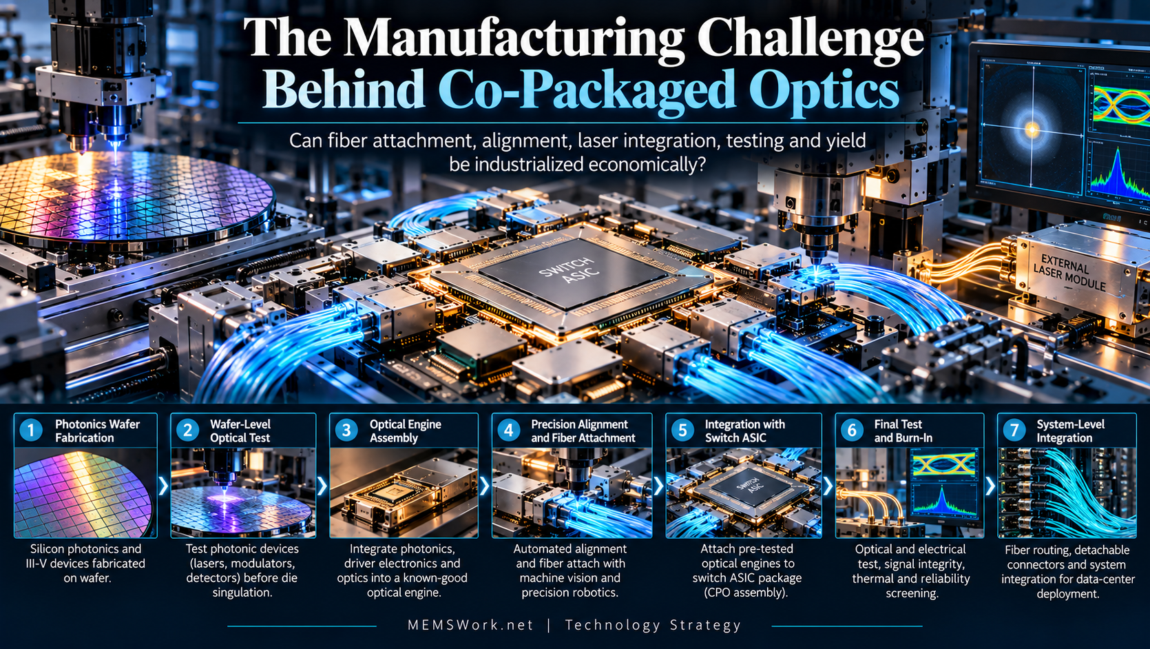
Can fiber attachment, alignment, laser integration, testing and yield be industrialized economically?
Co-packaged optics has moved beyond a bandwidth demonstration. The decisive question is now industrial: can photonic engines, fibers, lasers and switch silicon be assembled with semiconductor-like repeatability, test coverage and repair economics? The manufacturing bottleneck is shifting toward earlier defect detection, automated alignment, external-laser architectures, standardized fiber interfaces and OSAT-compatible process flows.
Executive Summary
AI infrastructure spending is forcing optical interconnect from laboratory programs into real manufacturing decisions. Microsoft reported $41 billion of quarterly capital expenditure in its June 2026 quarter, while Broadcom reported $16.7 billion of AI semiconductor revenue in fiscal Q3 2026, up 221% year over year [1][2]. That demand is pulling co-packaged optics (CPO) toward volume deployment—but optical bandwidth is no longer the most difficult question.
The tougher problem is how to manufacture CPO economically. Broadcom says its second-generation Tomahawk 5-Bailly became the industry’s first volume-production CPO solution, with learning concentrated in automated test, OSAT processes, fiber routing, thermal design, handling and yield [3]. NVIDIA’s Spectrum-X Photonics architecture similarly emphasizes automated final-stage fiber attachment and pre-tested, solder-reflow-compatible optical engines so that only known-good engines are attached to valuable switch silicon [4]. TSMC says COUPE-on-substrate co-packaged optics begins production in 2026 [5]. These are manufacturing milestones, not merely optical roadmaps.
Key Findings
| Manufacturing gate | Why it becomes a bottleneck | What can improve economics |
|---|---|---|
| Fiber attach / alignment | Optical loss is sensitive to placement, contamination and package movement. | Passive/surface-normal coupling, machine vision, precision robotics, standardized connectors. |
| Optical-engine yield | A late defect can strand expensive switch silicon and advanced packaging. | Wafer-level test, known-good engines, hierarchical screening before final integration. |
| Laser architecture | Lasers add heat, lifetime and replacement risk near the switch ASIC. | External laser modules, redundancy and field-replaceable ELSFP architectures. |
| Final test / burn-in | Optical, electrical and thermal interactions must be qualified together. | Automated optical test, built-in test features, reliability analytics and OSAT-compatible flows. |
1. The Bottleneck Has Shifted From Photonic Performance to Manufacturing Yield
The case for moving optics closer to the switch ASIC is already strong: shorter electrical paths can reduce power and improve bandwidth density. But CPO changes the unit of manufacturing risk. Instead of replacing a failed pluggable optical module at the front panel, manufacturers combine switch silicon, photonic engines, advanced packaging, fibers and laser infrastructure into a tightly coupled system. A defect discovered late can therefore destroy more accumulated value.
Broadcom’s manufacturing history is instructive. The company describes first-generation CPO as a supply-chain learning vehicle; its second-generation TH5-Bailly then moved into volume production, with improvements in OSAT process maturity, thermal design, handling, fiber routing, automated testing and overall yield. Its third-generation platform now operates at 200 Gb/s per lane [3]. The strategic transition is therefore from proving optical performance to controlling process variation.
Where CPO Yield Can Be Lost—and Protected
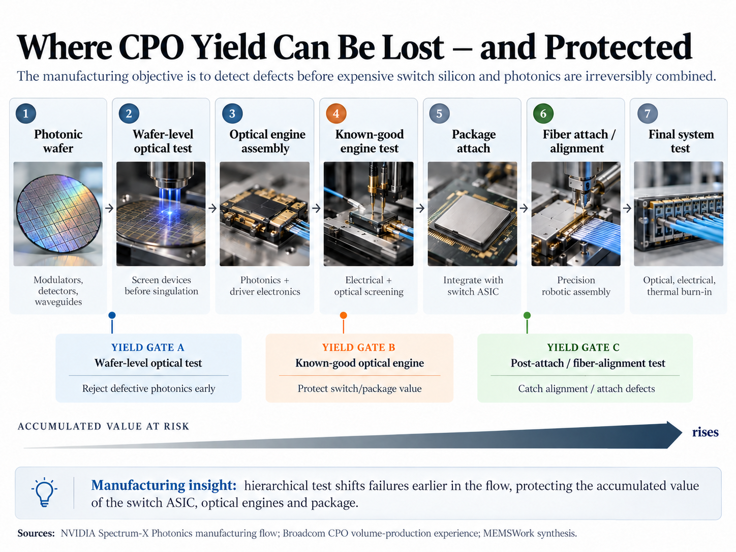
Figure 1. Where CPO yield can be lost—and protected. Hierarchical test shifts failure discovery earlier in the manufacturing flow, reducing the risk that a defective optical engine or fiber interface destroys the accumulated value of the switch ASIC and package. Sources: NVIDIA [4], Broadcom [3]; MEMSWork synthesis.
2. Fiber Attachment and Alignment Must Become Manufacturing Processes
Photonics introduces a manufacturing problem that digital semiconductor assembly largely avoids: light must couple efficiently between structures that can be sensitive to micron-scale placement error, contamination and thermal movement. Any assembly step that requires slow active alignment can become a throughput constraint when thousands or millions of optical ports are required.
NVIDIA is attacking this by moving fiber attachment to the final manufacturing stage and using surface-normal optical I/O compatible with automated precision equipment. It also designs the optical engine to survive standard solder-reflow assembly so the engine can be screened before attachment [4]. Broadcom similarly highlights detachable fiber connectors, automated testing and improved fiber routing as elements of its CPO manufacturing maturity [3]. The industrialization goal is straightforward: replace operator-dependent precision work with characterized equipment, standardized interfaces and process windows that can be monitored statistically.
From Precision Photonics Assembly to Semiconductor Manufacturing
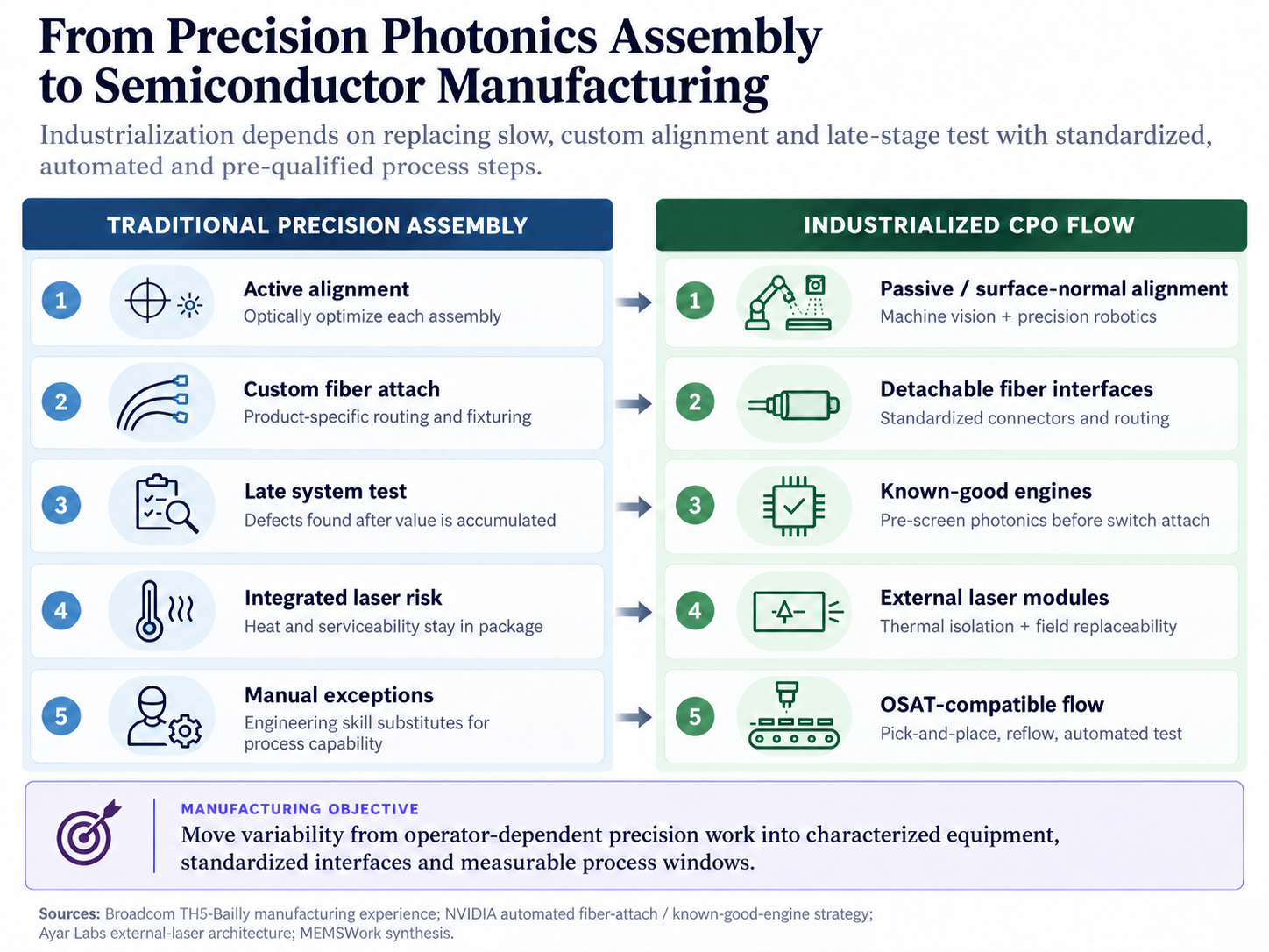
Figure 2. From precision photonics assembly to semiconductor manufacturing. The economic transition depends on automation, pre-qualified optical engines, standardized fiber interfaces, external lasers and OSAT-compatible process steps. Sources: Broadcom [3], NVIDIA [4], Ayar Labs [7]; MEMSWork synthesis.
3. Laser Integration Is a Reliability and Serviceability Decision
More integration is not automatically better. Efficient laser sources commonly use III-V materials and introduce heat, aging and replacement concerns. Putting the laser immediately beside an expensive switch ASIC can simplify the optical path but complicate field service if the laser fails.
That is why several architectures externalize the light source. Ayar Labs’ SuperNova external laser is packaged in the industry-standard ELSFP form factor and is designed to be field-replaceable; Ayar says separating the laser from its TeraPHY optical engines improves thermal efficiency, reliability and serviceability [7]. Lumentum is investing upstream in this architecture: its new 240,000-square-foot North Carolina facility is being converted to manufacture InP continuous-wave and ultra-high-power lasers for AI optical systems [8]. Lumentum’s fiscal Q4 2026 revenue reached $1.01 billion, up from $480.7 million a year earlier, while management specifically cited increasing demand for ultra-high-power CPO lasers, initial external-laser-module orders and near-package-optics activity [9].
Capital and Production Milestones Are Moving CPO Toward Industrial Scale
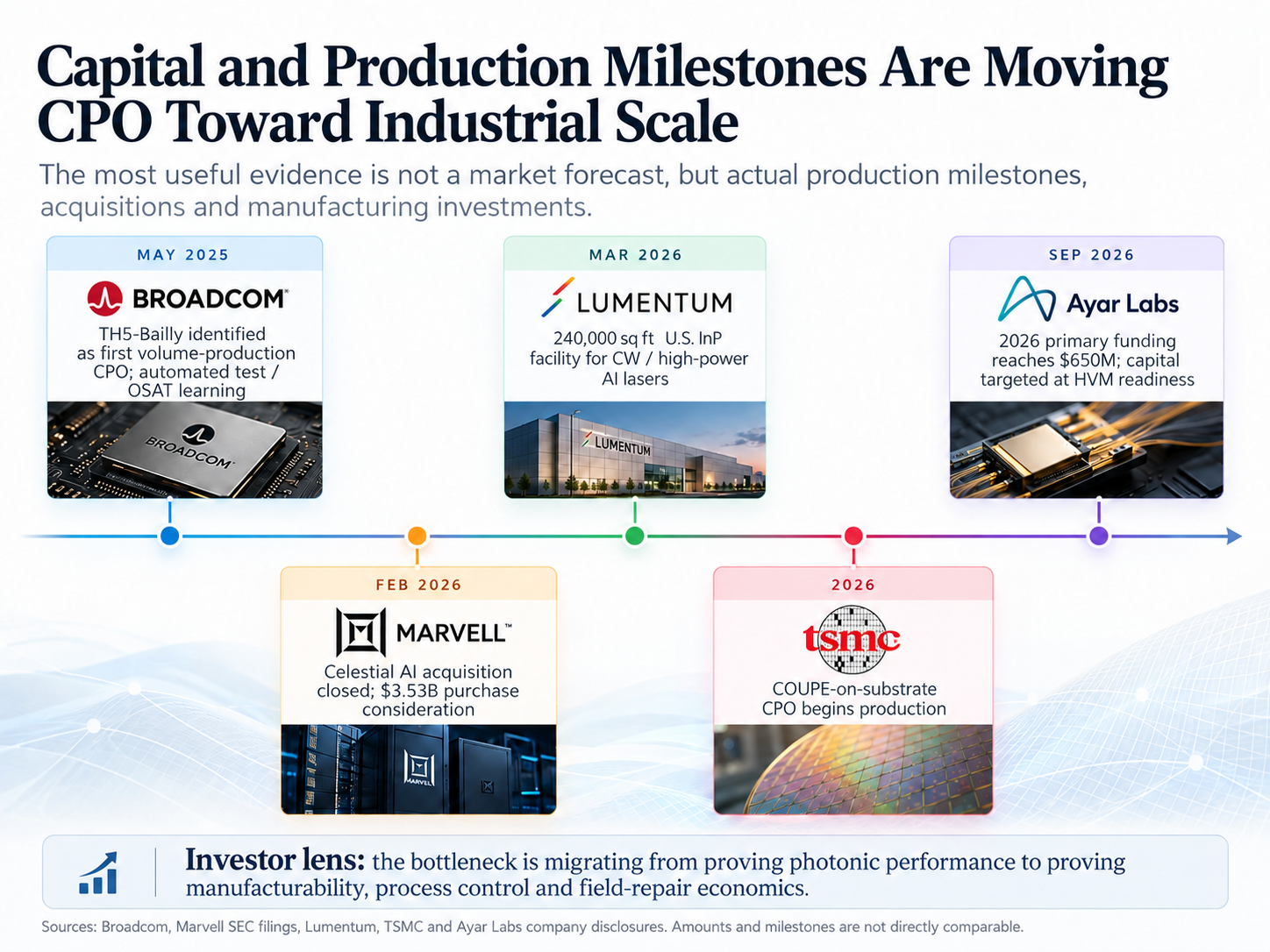
Figure 3. Capital and production milestones are moving CPO toward industrial scale. The evidence spans volume production, foundry production, laser capacity, acquisitions and high-volume-manufacturing funding; the items are not directly comparable. Sources: Broadcom [3], Marvell [11], Lumentum [8], TSMC [5], Ayar Labs [10].
Laser Architecture Is a Manufacturing and Serviceability Tradeoff
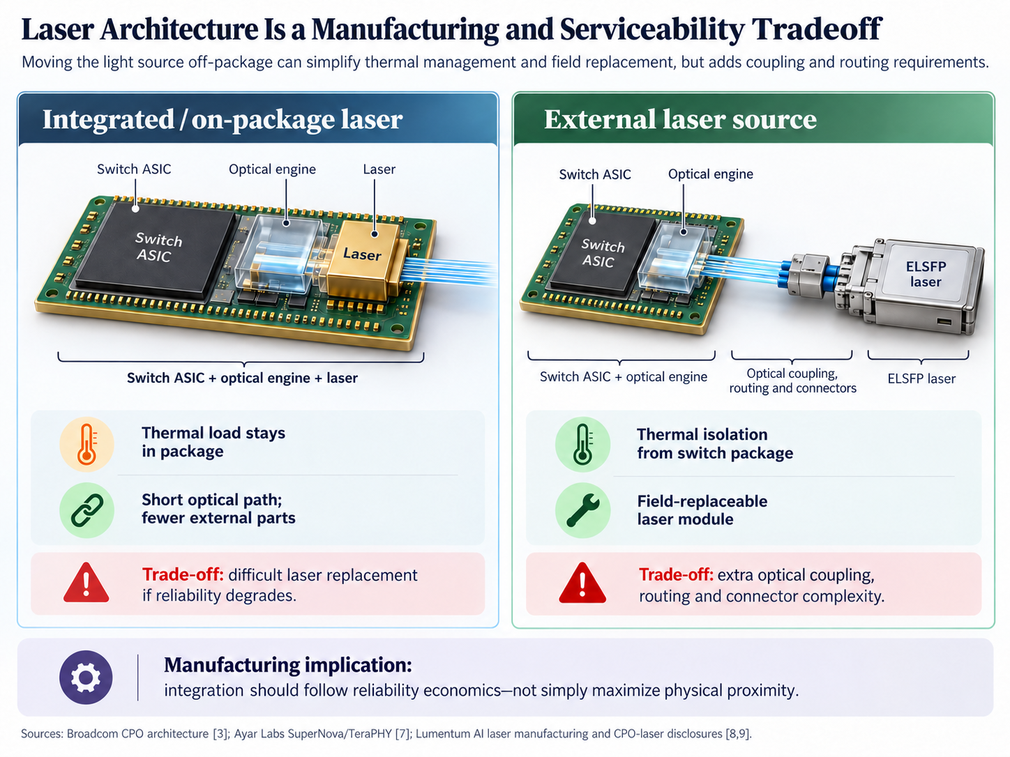
Figure 4. Integrated versus external laser-source architectures. Externalizing the laser can improve thermal isolation and field replaceability, while on-package integration shortens the optical path but increases replacement and thermal coupling risk. Sources: Broadcom CPO architecture [3]; Ayar Labs SuperNova/TeraPHY [7]; Lumentum AI-laser manufacturing and CPO-laser disclosures [8] [9].
4. Known-Good Optical Engines May Be the Most Important Yield Lever
The core manufacturing principle is hierarchical test. Rather than assemble the entire switch and discover failures at final test, suppliers need to identify defects at the wafer, optical-engine, laser and package levels before more value is added. NVIDIA says its solder-reflow-compatible optical engines can be fully screened before attachment; the company describes this as guaranteeing 100% yield at the optical-engine integration step. That should be read narrowly as a vendor manufacturing claim for the screened-engine attach step—not as a claim of 100% overall CPO-system yield [4].
This distinction matters economically. A CPO switch may combine a costly switch ASIC with multiple optical engines and advanced packaging. The earlier a defective engine is detected, the less valuable material and assembly time is scrapped. That creates a market for wafer-level optical probing, automated coupling equipment, built-in self-test, machine vision, thermal/reliability screening and manufacturing analytics.
The Economic Cost of a Defect Rises as CPO Assembly Progresses
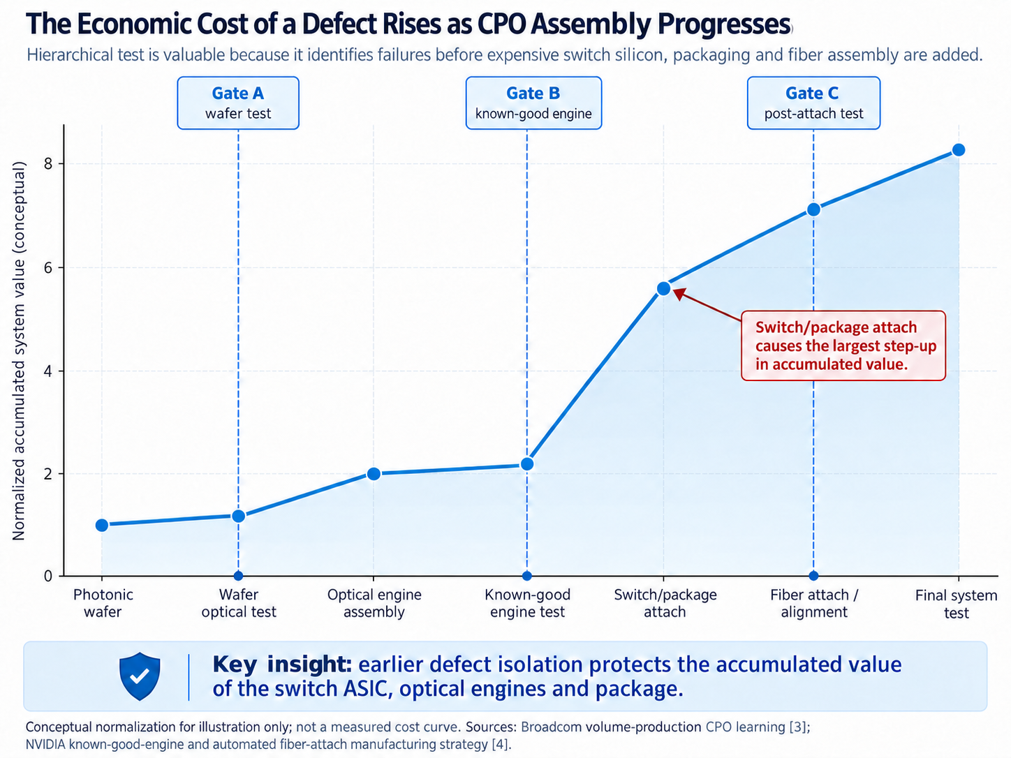
Figure 5. Conceptual accumulation of system value through the CPO manufacturing flow. The curve is illustrative rather than measured; it shows why earlier defect isolation can protect the value of the switch ASIC, optical engines, packaging and fiber assembly. Sources: Broadcom volume-production CPO learning [3]; NVIDIA known-good-engine and automated fiber-attach manufacturing strategy [4].
5. The Foundry and OSAT Stack Is Moving In
TSMC’s involvement is a major industrialization signal because it brings silicon photonics into an established advanced-packaging ecosystem. At its 2026 Technology Symposium, TSMC said COUPE-on-substrate production begins in 2026 and cited 2× power efficiency and 10× lower latency versus a pluggable implementation on the circuit board; those performance figures are TSMC comparisons rather than independent benchmarks [5]. Its 2025 annual report also says CoWoS CPO is under development to combine interposer-based compute modules with COUPE optical I/O [6].
Capital is following the same manufacturing problem. Ayar Labs raised $650 million of primary capital in 2026, explicitly directing the funding toward manufacturing-ecosystem readiness and high-volume production [10]. Marvell completed its Celestial AI acquisition in February 2026 for total purchase consideration of approximately $3.53 billion, giving the company a Photonic Fabric platform intended for next-generation scale-up interconnect [11]. These investments do not prove that CPO economics are solved, but they show that strategic capital is moving toward manufacturing and integration capability rather than photonic devices alone.
6. Where the Constraint Gets Solved—and Where Investment Opportunities Emerge
| Constraint | Near-term solution | Innovation opportunity | Strategic exposure |
|---|---|---|---|
| Alignment / fiber attach | Passive or surface-normal coupling; automated precision placement | Machine vision, robotics, metrology, detachable fiber connectors | Assembly-equipment and precision-photonics suppliers |
| Optical-engine yield | Wafer-level test and known-good-engine screening | Optical probes, built-in self-test, high-throughput optical test | Test and measurement / OSAT ecosystem |
| Laser reliability | External laser modules and redundancy | High-power CW lasers, ELSFP modules, laser health monitoring | Lumentum and specialty InP suppliers |
| Package integration | Reflow-compatible engines and standardized assembly | Photonics packaging, substrates, thermal co-design | Foundries, OSATs, packaging equipment |
| Process variability | Statistical process control and design-for-manufacture | Yield analytics, digital twins, electro-optical co-simulation | EDA / manufacturing software |
Table 1. CPO manufacturing constraints, near-term solutions, innovation opportunities and strategic exposure. MEMSWork synthesis based on company manufacturing, packaging, test and laser-source disclosures [3] [4] [5] [6] [7] [8] [9] [10] [11].
7. What Could Delay the Manufacturing Curve?
CPO still faces meaningful execution risk. Pluggable optics retains a deep, interoperable service ecosystem. Passive copper and active electrical cables continue improving at short reach. CPO package failures can be more expensive to diagnose or repair, and standardized field-service models are still developing. Even if photonic devices work well, the commercial crossover can be delayed if assembly yield, fiber repair, laser replacement, burn-in time or package rework remain too costly.
That is why the next useful evidence is operational rather than promotional: disclosed volume yields, automated alignment cycle times, optical-engine failure rates, field laser replacement rates, repair workflows and adoption across multiple system vendors. A product being “in production” is important, but broad infrastructure adoption requires repeatable economics outside tightly controlled reference platforms.
Investor Takeaway
The technology case for co-packaged optics is increasingly credible; the manufacturing case is still being proven. The decisive value may therefore migrate toward the companies that make photonics behave more like semiconductor manufacturing: automated fiber attach, passive alignment, known-good-engine test, high-power external lasers, advanced packaging, metrology and statistical yield control. The winners may not simply be the companies with the best photonic devices. They may be the companies that make photonics manufacturable at AI scale.
References
[1] Microsoft, FY2026 Q4 Earnings Conference Call, July 29, 2026.
[2] Broadcom, Q3 FY2026 Financial Results, Sept. 2, 2026.
[4] NVIDIA, Scaling Power-Efficient AI Factories with Spectrum-X Ethernet Photonics, Jan. 6, 2026.
[5] TSMC, 2026 North America Technology Symposium: COUPE-on-substrate production milestone.
[6] TSMC, 2025 Annual Report: COUPE and CoWoS CPO development.
[7] Ayar Labs, SuperNova External Light Source / TeraPHY optical engine.
[8] Lumentum, New U.S. Manufacturing Facility for Advanced AI Lasers, Mar. 26, 2026.
[9] Lumentum, Q4 and FY2026 Results, Aug. 11, 2026.
[10] Ayar Labs, 2026 Funding Expanded to $650 Million, Sept. 10, 2026.
[11] Marvell, Q2 FY2027 Form 10-Q: Celestial AI purchase consideration, Aug. 28, 2026.
Research note: Vendor performance and manufacturing claims are identified as such. Corporate investment and transaction figures are drawn from company disclosures and SEC filings. This report is strategic research, not investment advice.