AI’s Next Packaging Bottleneck: Qualifying the Supplier Ecosystem
AI-chip output depends on more than advanced-packaging floor space. Equipment, materials, metrology and reliability methods must be qualified together before new capacity becomes repeatable production. Taiwan’s new Baipu supplier cluster makes that hidden constraint visible—and offers a useful test of whether co-location can compress learning cycles without sacrificing yield discipline.
Taiwan broke ground in September 2026 on the Baipu Industrial Park in Kaohsiung, positioning it as a cluster for advanced-packaging equipment and materials suppliers. Taiwan’s Ministry of Economic Affairs said the park will emphasize research and development, inspection and verification, and the introduction of critical equipment into production. The policy aim is not merely to add factory buildings; it is to connect suppliers more directly to the advanced logic and packaging activity developing in southern Taiwan. [1]
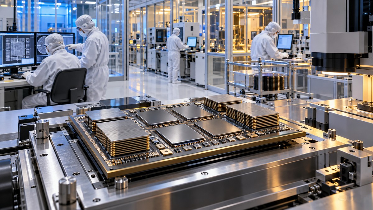
That distinction matters because advanced packaging is increasingly part of the computing architecture. TSMC describes CoWoS as a platform that integrates logic dies with high-bandwidth memory through an interposer or redistribution structure. Its current CoWoS-S offering supports interposers up to about 3.3 times reticle size, while CoWoS-L and CoWoS-R extend the design space for larger systems. [2] As packages expand, the number of interfaces, materials and process steps grows—and so does the number of ways a nominal capacity expansion can fail to become saleable output.
The constraint is qualification, not just square footage
A new tool or material cannot move directly from a supplier demonstration into a high-volume AI package. It must fit the process flow, meet dimensional and contamination requirements, survive reliability testing, generate interpretable metrology data and perform consistently across production lots. A promising laboratory result may still fail because of warpage, bonding defects, thermal gradients, particle sensitivity, throughput limits or an unstable process window.
SEMICON Taiwan’s 2026 advanced-testing program framed the same problem from the test side: chiplets, HBM and higher-power systems require test to connect more closely across design, manufacturing and system-level validation. One technical session highlighted growing package footprints, severe thermal gradients, more complicated yield learning and test costs that rise with device size, test time and system validation. [3] [4] Those are operational constraints, not reasons the technology cannot scale. They do mean that announced equipment and floor space should not be counted as productive capacity until customer qualification and yield evidence follow.
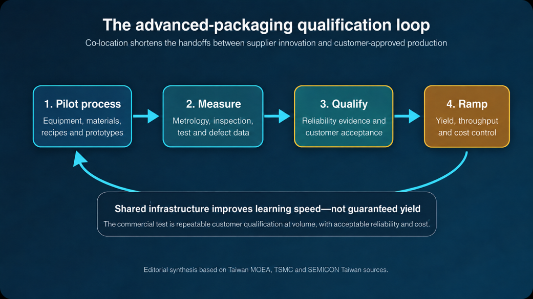
Figure 1. Advanced-packaging supplier qualification is an iterative loop: pilot processes generate inspection and test data, customer reliability requirements determine acceptance, and volume-ramp results feed back into recipes and equipment. Co-location can shorten handoffs, but it does not guarantee yield. Editorial synthesis based on Taiwan MOEA, TSMC and SEMICON Taiwan sources. [1] [5] [4]
Why the package roadmap raises the stakes
TSMC’s 2026 technology roadmap shows why qualification must accelerate. The company said it was producing 5.5-reticle-size CoWoS and plans a 14-reticle-size version for production in 2028, designed to integrate approximately 10 large compute dies and 20 HBM stacks. TSMC also described expansion beyond 14 reticles in 2029 and a 40-reticle-size system-on-wafer offering expected that year. These are company roadmaps rather than independently verified future output, but they make the direction clear: package scale and system complexity are rising rapidly. [5]
Larger assemblies amplify cumulative yield risk. If one expensive component, bond or interconnect fails late in the flow, the loss can include the value already embedded in multiple known-good dies and memory stacks. This shifts economic attention toward earlier defect discovery, better process control, repair or redundancy where feasible, and test strategies that identify problems before the highest-value assembly steps. The useful metric is therefore not packages started; it is qualified good packages shipped per unit of time and capital.
What a supplier cluster can change
Physical proximity can reduce the delay between a tool excursion, material change and engineering response. Suppliers can test revisions near customer process teams, compare measurements against a common reference flow and learn from production-relevant failure modes. A nearby training center can also shorten the path from equipment installation to competent operation. Reuters reported that TSMC plans a technology-validation laboratory and a talent-training center at Baipu, with operations targeted for the fourth quarter of 2029. That is a planned milestone, not current operating capacity. [6]
The cluster could particularly benefit smaller equipment and materials companies. Without shared or customer-adjacent validation access, a supplier may need to fund specialized tools, wait for scarce line time and repeat tests across incompatible environments. A cluster cannot remove intellectual-property boundaries or commercial competition, but common infrastructure and agreed measurement methods can reduce duplicated work. SEMICON Taiwan described digital twins, software-based control and co-creation as ways to improve precision, yield and time to market in advanced-packaging equipment. [7]
The evidence investors should demand
| Claim | Operating evidence | Why it matters |
|---|---|---|
| Faster supplier qualification | Time from pilot tool installation to customer acceptance; number of qualified recipes | Shows whether proximity actually shortens adoption cycles |
| Better manufacturing economics | Package yield, rework, scrap, test time and throughput | Separates productive capacity from installed capacity |
| Supply-chain resilience | Second-source approvals, local spare-part coverage and material lead times | Tests whether the cluster reduces dependency rather than merely relocating it |
| Scalable technology | Reliability results across lots, package sizes and customer products | Prevents a successful demonstration from being mistaken for a repeatable platform |
Table 1. Proposed indicators for evaluating advanced-packaging supplier clusters. These are editorial assessment criteria, not forecasts. They are derived from the qualification and scaling issues described by TSMC, Taiwan MOEA and SEMICON Taiwan. [2] [3] [7]
Policy support should be judged by the same evidence. Land, buildings and incentives can attract suppliers, but a durable cluster also needs utilities, technical talent, shared standards, protection of proprietary process knowledge and enough customer demand to keep pilot and validation resources utilized. The September groundbreaking is therefore an input. The outcome will be visible later in qualification speed, yield learning and supplier adoption.
Strategic implications
For semiconductor equipment and materials suppliers, the opportunity is to become part of the customer’s learning loop rather than sell a stand-alone tool. Metrology, automated inspection, advanced bonding, thermal-interface materials, substrates, contamination control and data systems all become more valuable when they reduce qualification time or protect the accumulated value of a complex package. Panel-level approaches and glass-based architectures may widen the future equipment opportunity, but SEMICON Taiwan’s commercialization discussion emphasizes that fine-line redistribution, new materials and high-precision processing must advance together. [8]
For investors and corporate strategists, the central question is not whether advanced packaging is important; that is already evident in the architecture of leading AI systems. The sharper question is which companies can convert tighter supplier–customer feedback into qualified, repeatable output. Baipu is strategically interesting because it treats validation infrastructure and supplier integration as capacity. If the model works, the payoff will not be the announcement of a larger park. It will be faster learning, more approved suppliers and a higher flow of reliable packages from the same capital base.
References
- Taiwan Ministry of Economic Affairs / Invest Taiwan, “Baipu Park Focuses on Advanced Semiconductor Packaging,” September 1, 2026.
- TSMC, “CoWoS®,” accessed September 25, 2026.
- SEMICON Taiwan, “Advanced Testing Forum 2026,” September 2026.
- SEMICON Taiwan, “Advancing Test to Enable Advanced Packaging Roadmaps,” September 2026.
- TSMC, “TSMC Debuts A13 Technology at 2026 North America Technology Symposium,” April 22, 2026.
- Reuters, “Taiwan breaks ground on advanced packaging park anchored by TSMC,” September 21, 2026.
- SEMICON Taiwan, “AI-Ready Equipment: Building Global Competitiveness in Advanced Packaging Equipment,” September 2026.
- SEMICON Taiwan, “Enabling the Next Era of Heterogeneous Integration with Panel-Level Packaging Innovation and Commercialization,” September 2026.