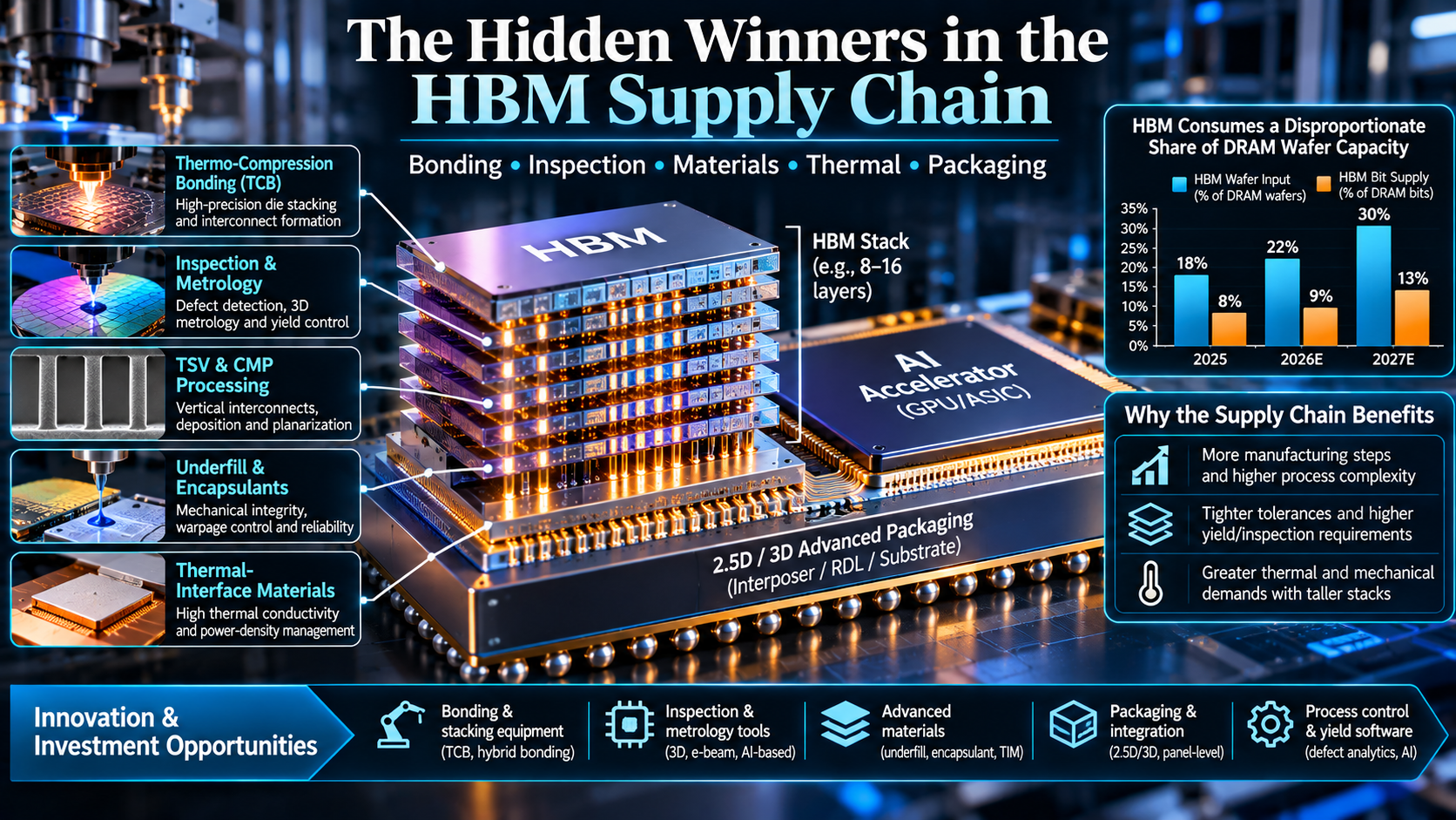
Image credit: MEMSWork (AI-assisted illustration).
Beyond the three major memory suppliers, HBM growth is creating a second layer of beneficiaries in bonding, inspection, process equipment, materials, thermal management and advanced packaging. The key investor question is which suppliers gain content as each HBM stack becomes taller, harder to manufacture and more valuable.
Executive Summary
HBM is not simply a faster version of conventional DRAM. It requires larger die area, through-silicon vias (TSVs), wafer thinning, precision stacking, thermocompression bonding, inspection, encapsulation, thermal management and advanced package integration. That manufacturing intensity creates a supplier opportunity that can grow faster than HBM bit shipments themselves.
TrendForce estimates that HBM will consume about 18%, 22% and 30% of total DRAM wafer input among the three leading suppliers at the end of 2025, 2026 and 2027, respectively, while representing only about 8%, 9% and 13% of DRAM bit supply [1]. In other words, HBM consumes roughly 2.3 times as much wafer share as bit share across those estimates. For equipment and materials suppliers, that is the central economic signal: HBM creates more manufacturing content per delivered bit.
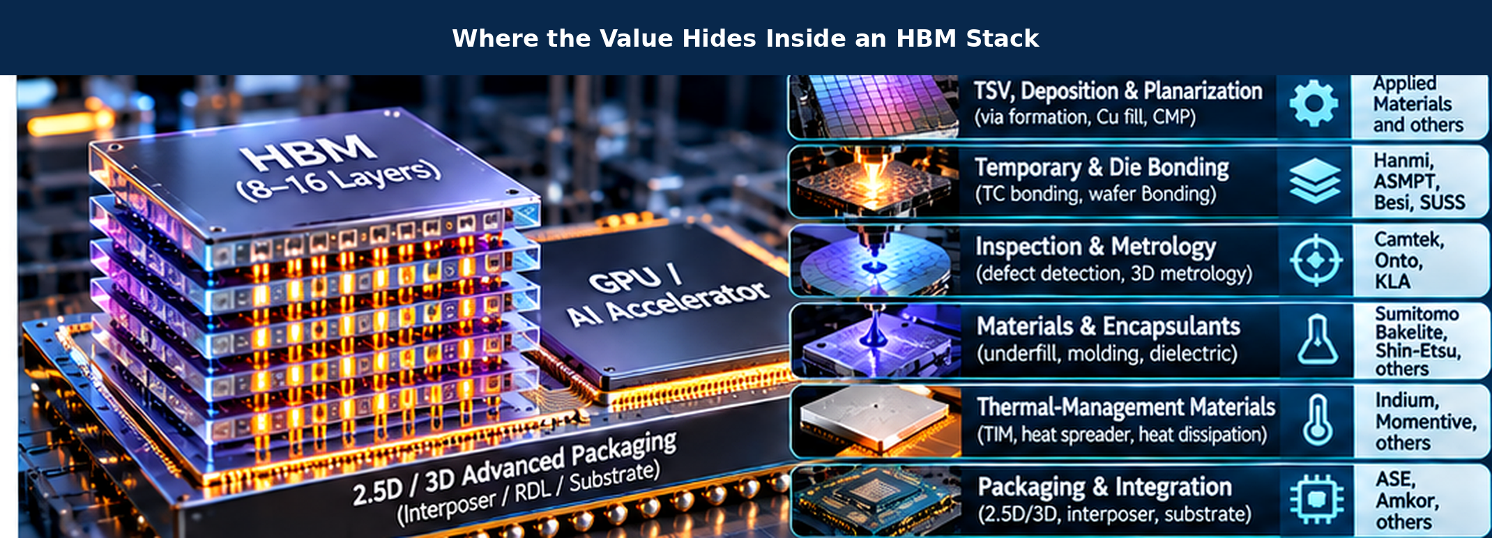
Figure 1. Where the value hides inside an HBM stack. Each additional layer raises requirements for bonding precision, process control, advanced materials and downstream package integration. Sources: Camtek [3], Onto Innovation [4], Applied Materials [5], Sumitomo Bakelite [8–9], ASE [10]; MEMSWork synthesis.
1. Bonding Is the First Visible Picks-and-Shovels Opportunity
HBM is fundamentally a stacked-memory product, making bonding equipment one of the clearest current beneficiaries. In June 2026, SK hynix ordered KRW 44.2 billion (about US$28.7 million) of Hanmi Semiconductor thermocompression bonders for next-generation HBM4 production [2]. The order is strategically important because it ties HBM capacity expansion directly to a specialized equipment supplier rather than to memory wafers alone.
ASMPT is attacking the same bottleneck with AOR TCB, a fluxless thermocompression-bonding process that removes oxides during bonding and is intended to support finer pitches, cleaner interfaces and higher-density stacking [6]. For investors, the useful distinction is between technologies already generating HBM-related orders and those that remain optionality. Conventional TCB is still being extended aggressively, while SUSS MicroTec said in its Q3 2026 call that it does not yet see mass adoption of hybrid bonding for HBM [12].
2. Inspection and Metrology Become More Valuable as the Stack Becomes More Expensive
Inspection may be an even more attractive content-per-stack story because the economic cost of a late defect rises with every processed die added to the stack. Camtek disclosed more than $50 million of Hawk-system orders from a leading HBM manufacturer in June 2026, alongside a $55 million order from a Tier-1 OSAT supporting AI applications [3]. Onto Innovation was later named SK hynix’s 2026 Best Partner for technology achievement after developing measurement technology aimed at hidden HBM defects [4].
The technical reason is straightforward. Moving from lower stack counts toward 12-high and 16-high HBM requires thinner dies and more assembly steps, increasing the risk of cracks, sub-surface defects and bonding failures [4]. KLA’s fiscal 2026 annual report similarly identified HBM and advanced packaging as drivers of more demanding inspection, metrology and yield-optimization requirements; KLA generated $13.58 billion of fiscal 2026 revenue while describing AI-driven process-control demand as a structural growth driver [7].
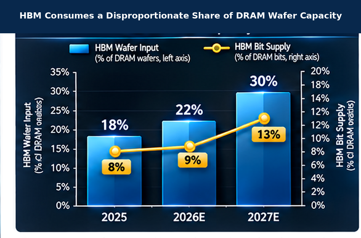
Figure 2. HBM consumes a disproportionate share of DRAM wafer capacity. TrendForce estimates HBM wafer input at 18%, 22% and 30% of total DRAM wafer input in 2025–2027 versus only 8%, 9% and 13% of DRAM bit supply. Source: TrendForce [1].
3. Process Equipment and Materials Gain Content Per Stack
TSVs, copper interconnects and tighter package tolerances create another layer of beneficiaries. Applied Materials introduced new CMP, deposition and e-beam systems in June 2026 specifically targeting DRAM, HBM and advanced packaging [5]. The company notes that it already supplies equipment covering many of the materials-engineering steps needed to create TSVs, copper pillars and microbumps. As layer counts rise, surface planarity and defect control become increasingly important because the next bonding step inherits every upstream non-uniformity.
Materials face a similar complexity multiplier. Sumitomo Bakelite’s semiconductor roadmap explicitly includes HBM encapsulants, molded underfill, high-thermal-conductivity TIMs and organic hybrid-bonding materials [8]. In October 2026, the company announced new production lines in China and Singapore for advanced-package mold-underfill and compression-molding materials as packages become denser, thinner and larger [9]. These materials are not glamorous, but they determine gap filling, warpage, adhesion, stress and thermal reliability.
4. Packaging Turns HBM Supply Into Deployable AI Compute
HBM is manufactured by the memory suppliers, but its economic value is realized only when it is integrated beside a GPU or custom accelerator. ASE’s automated 310 mm × 310 mm panel-level packaging line, scheduled for production in 2027, is explicitly aimed at increasingly large heterogeneous systems combining logic, chiplets and HBM [10]. SK hynix is also investing more than $4 billion in Indiana for a U.S. HBM advanced-packaging and production base, with next-generation HBM mass production targeted for the second half of 2029 [11].
Thermal materials sit at the same intersection. Taller stacks and higher-power accelerators create larger heat fluxes and more difficult warpage conditions. Indium Corporation is developing high-conductivity metal thermal-interface materials for large AI/HPC packages, highlighting the transition from conventional polymer TIMs toward materials engineered for much higher thermal design power [13].
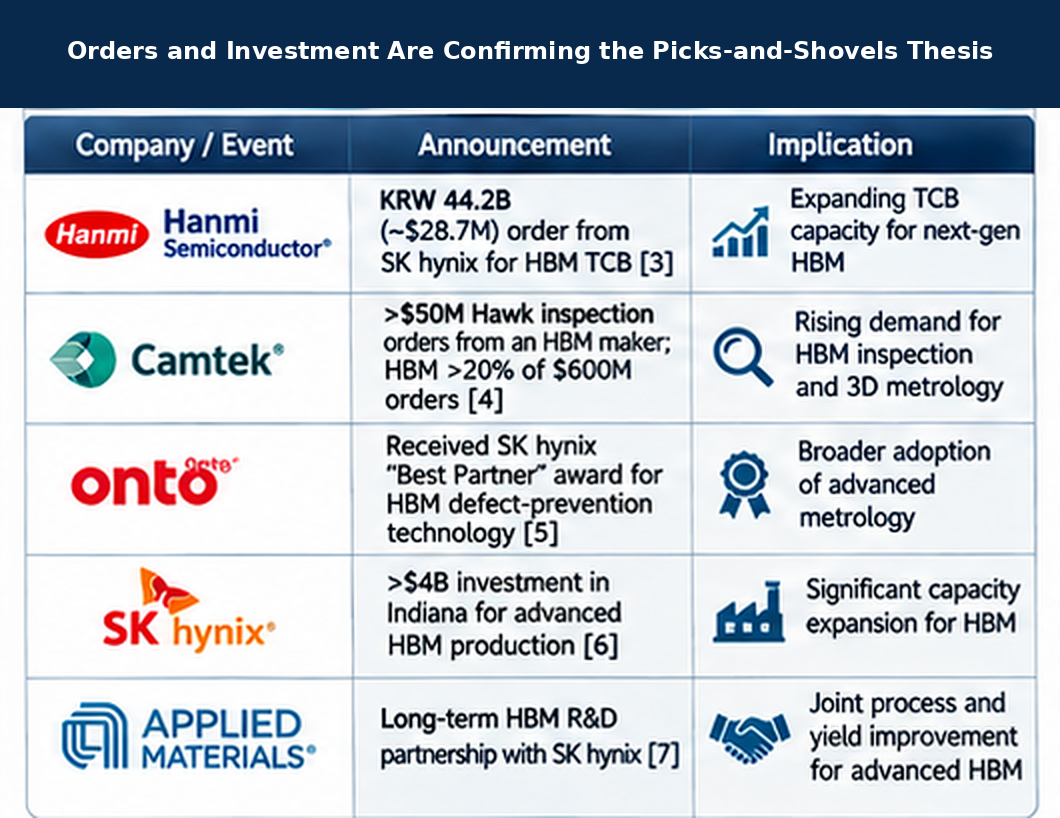
Figure 3. Disclosed orders and capital commitments already support the HBM picks-and-shovels thesis. Sources: Hanmi/SK hynix [2], Camtek [3], Applied Materials [5], Onto Innovation [4], Sumitomo Bakelite [9] and SK hynix [11].
5. How the Bottlenecks Get Relieved
The first solution is throughput: more TCB tools, inspection capacity, TSV/CMP equipment and packaging lines. The second is yield. Earlier optical and electrical defect detection, known-good-die selection, better warpage control and tighter process analytics can convert the same installed wafer capacity into more saleable HBM stacks. The third is material innovation: lower-stress encapsulants, improved thermal interfaces and finer-pitch interconnect materials can extend current stacking methods before a wholesale process transition is required.
Hybrid bonding remains an important longer-term possibility because it can reduce interconnect pitch and potentially improve density and power. But it should not be treated as today’s HBM revenue base. SUSS MicroTec’s recent comments that HBM hybrid bonding is not yet in mass adoption are an important counterweight to the hype [12]. That makes current TCB, inspection and materials exposure analytically different from future hybrid-bonding optionality.
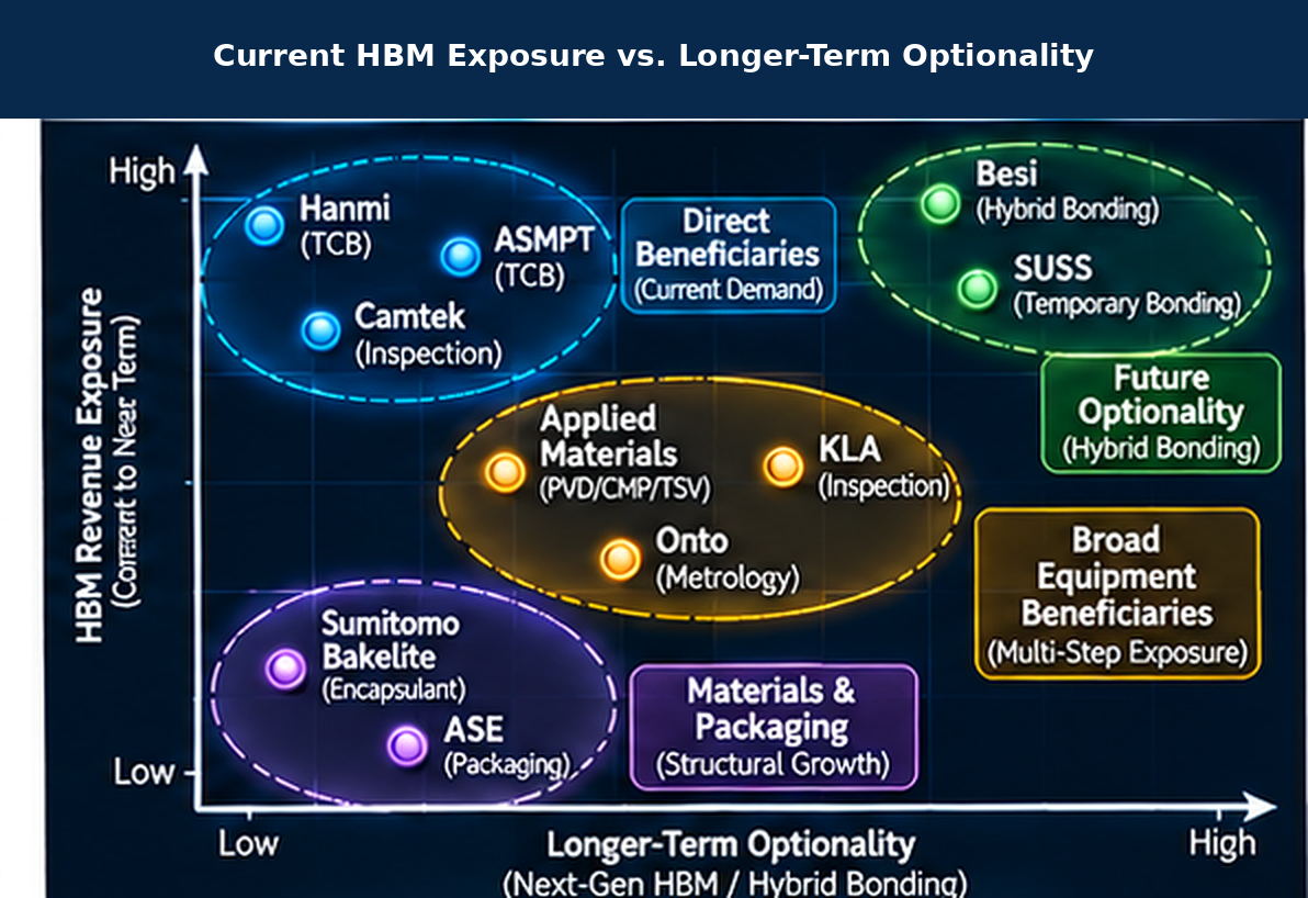
Figure 4. Current commercial exposure versus longer-term HBM optionality. TC bonding, inspection/metrology and process equipment already have visible HBM demand, while hybrid bonding remains a higher-leverage but less mature opportunity. Sources: Hanmi [2], ASMPT [6], Camtek [3], Onto [4], KLA [7], Applied Materials [5], ASE [10], SUSS MicroTec [12]. Positioning is qualitative MEMSWork synthesis, not a valuation ranking.
6. Innovation and Investment Opportunity Map
| Layer | Current bottleneck | Innovation opportunity | Representative exposure |
|---|---|---|---|
| Bonding | Stack height, pitch, residue, alignment | Higher-throughput TCB; fluxless bonding; hybrid bonding | Hanmi, ASMPT; Besi/SUSS optionality |
| Inspection / metrology | Hidden cracks, microbumps, late-stage yield loss | 3D metrology, e-beam review, AI defect analytics | Camtek, Onto, KLA |
| TSV / planarization | Uniformity and surface flatness | Improved CMP, deposition and process control | Applied Materials |
| Materials | Warpage, narrow-gap fill, thermal stress | MUF, low-stress encapsulants, high-k TIMs | Sumitomo Bakelite, specialty materials |
| Packaging | Large packages, cycle time, integration yield | Panel-level packaging, automation, design-for-test | ASE / OSAT ecosystem |
Table 1. HBM innovation and investment opportunity map. MEMSWork synthesis based on sources [2–13].
Investor Takeaway
The hidden HBM opportunity is not simply a collection of companies adjacent to AI. The strongest beneficiaries are suppliers whose revenue opportunity rises as each stack becomes harder to manufacture: more bonding steps, tighter inspection tolerances, more demanding planarization, better encapsulation and greater thermal-management requirements. That creates a different investment lens from choosing among SK hynix, Samsung and Micron.
The strategic question is therefore: which suppliers get paid regardless of which memory vendor wins share? Today, the clearest evidence sits in thermocompression bonding, inspection/metrology, process equipment and advanced materials. Hybrid bonding may eventually shift the value pool again, but the current revenue opportunity is already visible in customer orders, capacity expansion and supplier qualification.
References
[1] TrendForce, “Tight DRAM Supply Gives Suppliers Greater Pricing Power in HBM,” June 2, 2026.
https://www.trendforce.com/presscenter/news/20260602-13074.html
[2] Yonhap News Agency, “SK hynix orders new equipment worth 44.2 bln won for next-gen HBM4,” June 8, 2026.
https://en.yna.co.kr/view/AEN20260608012500320
[3] Camtek, “Camtek Receives Over $105 Million Multi-System Orders from a Tier-1 OSAT and a Leading HBM Manufacturer,” June 2, 2026.
https://www.camtek.com/news-and-events/camtek-receives-over-105-million-multi-system-orders-from-a-tier-1-osat-and-a-leading-hbm-manufacturer/
[4] Onto Innovation, “Best Partner Award from SK hynix for Hidden Defect Prevention in HBM Production,” Oct. 12, 2026.
https://investors.ontoinnovation.com/news/news-details/2026/Onto-Innovation-Receives-Best-Partner-Award-from-SK-hynix-for-Hidden-Defect-Prevention-in-High-Bandwidth-Memory-Production/default.aspx
[5] Applied Materials, “New Systems to Accelerate DRAM and Advanced Packaging for AI Chips,” June 25, 2026.
https://www.appliedmaterials.com/us/en/newsroom/press-releases/062526-applied-materials-introduces-new-systems-accelerate-dram-adv-pkg-ai-chips.html
[6] ASMPT, “Thermocompression Bonding with Active Oxide Removal,” May 28, 2026.
https://semi.asmpt.com/en/news-center/press-releases/thermocompression-bonding-with-active-oxide-removal/
[7] KLA Corporation, Fiscal 2026 Annual Report and Q4 FY2026 results. https://ir.kla.com/
[8] Sumitomo Bakelite, “Semiconductor Materials: Topics – Materials for AI Semiconductors,” 2025.
https://www.sumibe.co.jp/english/ir/library/presentation/files/2025/0512_04-2.pdf
[9] Sumitomo Bakelite, “Expansion of Production Capacity for Advanced Semiconductor Encapsulation Materials,” Oct. 9, 2026.
https://www.sumibe.co.jp/english/topics/2026/it-materials/1007_01/index.html
[10] ASE, “Automated 310mm Panel-Level Packaging to Accelerate AI Innovation,” May 26, 2026. https://ase.aseglobal.com/press-room/310×310/
[11] SK hynix, “Groundbreaking Ceremony for HBM Production Base in Indiana,” Aug. 28, 2026.
https://news.skhynix.com/en/groundbreaking-ceremony-in-indiana/
[12] SUSS MicroTec, Q3 2026 earnings call transcript, Nov. 4, 2026. https://stockanalysis.com/quote/etr/SMHN/transcripts/665672-q3-2026/
[13] Indium Corporation, “TIMs Solutions for AI Thermal Challenges at IMAPS ThermCon,” July 2, 2026. https://www.indium.com/press-releases/indium-corporation-expert-to-present-tims-solutions-for-ai-thermal-challenges-at-imaps-thermcon/
Research note: Forecasts and company statements are identified as such. Numerical corporate disclosures are sourced to primary company materials where available. The supplier positioning in Figure 4 and Table 1 is strategic analysis, not investment advice.