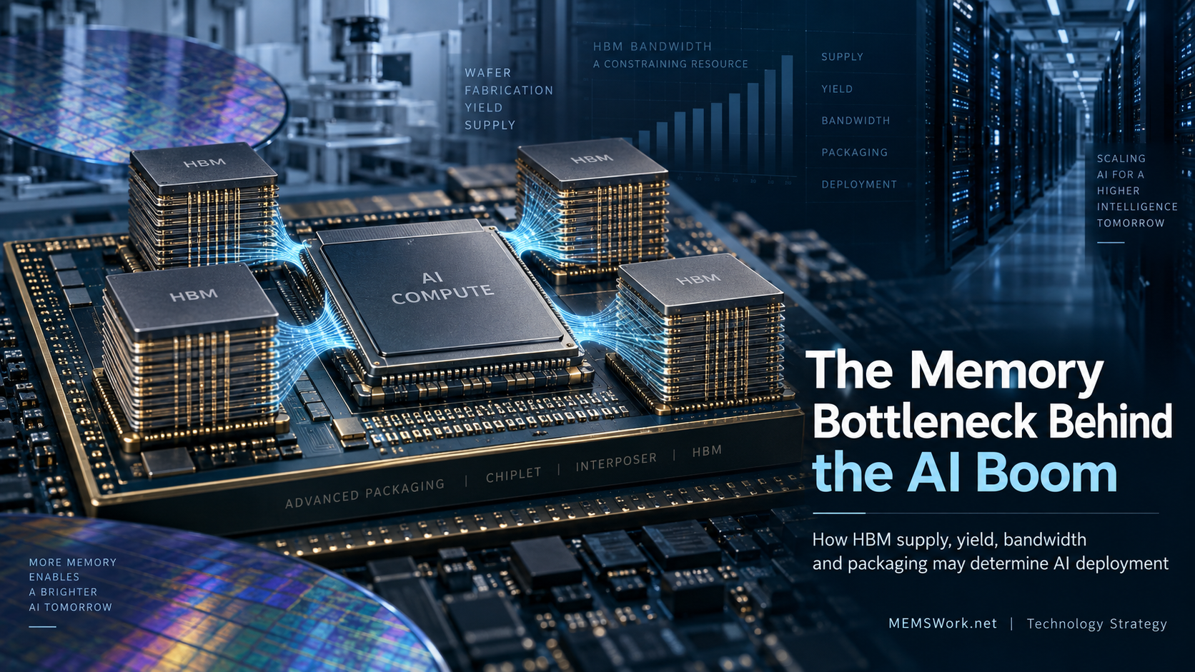
Concept illustration of the HBM and advanced-packaging constraint stack behind AI accelerators.
The Memory Bottleneck Behind the AI Boom
AI infrastructure is increasingly constrained not only by GPU supply, but also by high-bandwidth memory, advanced packaging, manufacturing yield, qualification, thermal management, and testing. These interconnected bottlenecks shape usable AI-compute capacity while creating new opportunities for technological innovation, strategic investment, and supply-chain development
Investors often track the AI infrastructure cycle through accelerator orders, data-center capital spending and the product roadmaps of NVIDIA, AMD and hyperscale cloud providers. But a finished GPU die is not deployable AI compute. It must be paired with enough high-bandwidth memory (HBM), pass electrical and thermal qualification, be integrated through advanced packaging and deliver enough bandwidth to keep increasingly powerful compute engines fed.
The economically relevant unit is therefore the complete accelerator package, not the logic die alone. This report examines where the constraint is moving, why nominal memory capacity differs from usable supply, how the bottleneck may be relieved and where investors and corporate planners should look for enabling innovation.
The bottleneck is moving beyond the GPU
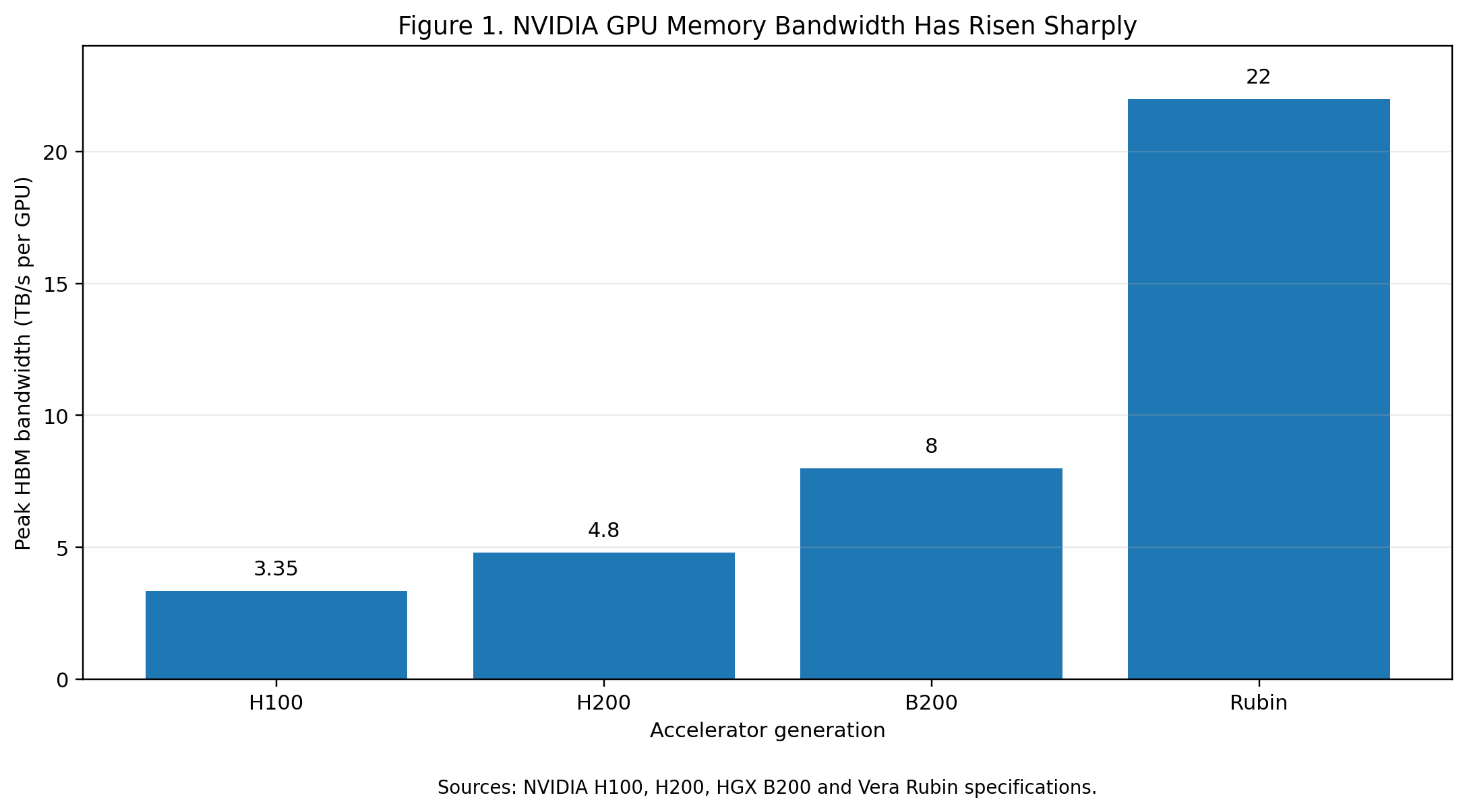
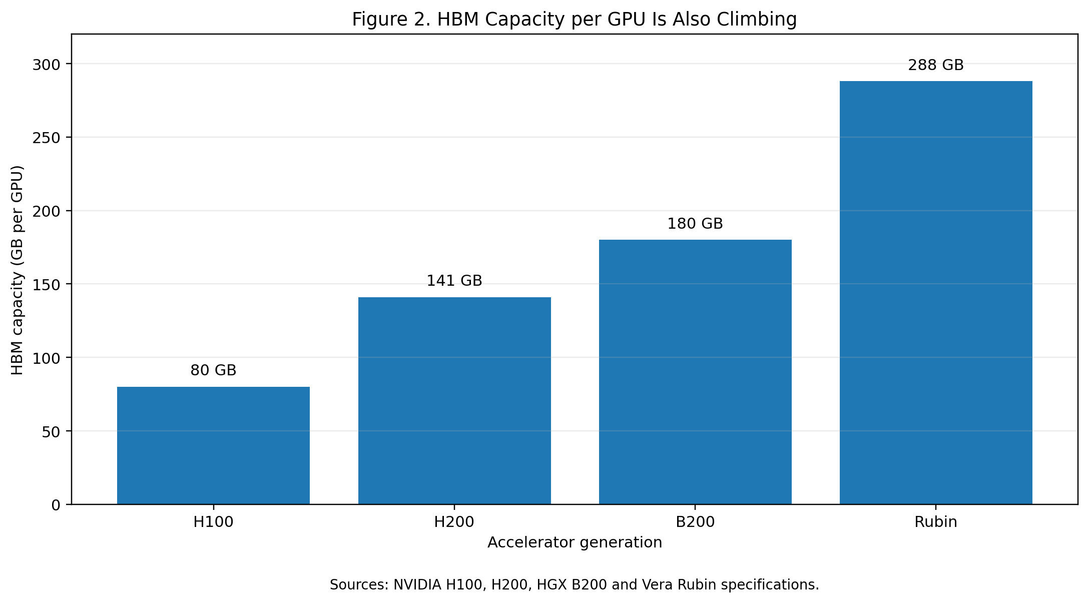
The direction of travel is visible in NVIDIA’s own specifications. H100 provides 80 GB of HBM3 and 3.35 TB/s of memory bandwidth; H200 increases that to 141 GB of HBM3e and 4.8 TB/s; B200 reaches 180 GB and as much as 8 TB/s; and Rubin moves to 288 GB of HBM4 and up to 22 TB/s. From H100 to Rubin, memory capacity rises 3.6 times while bandwidth rises about 6.6 times. AMD shows the same pattern: its MI455X lists 432 GB of HBM4 and 23.3 TB/s of peak memory bandwidth.
Why HBM is hard to scale
HBM is not simply conventional DRAM sold at a premium. It combines advanced memory fabrication with wafer thinning, through-silicon vias, vertical die stacking, fine-pitch interconnects, thermal control, testing and package integration. Micron’s current HBM4 uses a 2,048-pin interface at more than 11 Gb/s per pin and delivers more than 2.8 TB/s per stack. Its 12-high product provides 36 GB per stack; Micron states that HBM4 delivers more than twice the bandwidth of its HBM3E generation and more than 20% better power efficiency.
Those performance gains are strategically important because the value of an expensive accelerator falls if compute cores repeatedly wait for data. They also increase manufacturing difficulty. Supply is concentrated among SK hynix, Samsung Electronics and Micron, and these vendors must allocate wafer capacity and back-end resources among HBM, server DRAM and other products. TrendForce estimates that HBM plus RDIMM will consume 51% of DRAM bit supply in 2026 and forecasts a 70%-140% increase in HBM contract pricing for 2027 as tight supply and higher HBM4 manufacturing costs strengthen supplier pricing power. The forecast is not a certainty, but it illustrates the economic pressure created by AI demand.
Yield and qualification: nominal capacity is not usable capacity
HBM availability cannot be inferred from wafer starts alone. Each additional stacked die introduces another opportunity for defects, bonding problems, thermal variation or test loss. Defects late in the flow are especially costly because more accumulated value is destroyed. The relevant metric is therefore not installed capacity but the yield of known-good, qualified stacks that can be assembled into accelerator packages.
Qualification adds a second gating factor. A stack that functions in isolation is not commercially useful until it meets the target accelerator platform’s signal-integrity, power, thermal, timing and reliability requirements. SK hynix reported beginning HBM4 mass shipments in the second quarter of 2026 and highlighted high yield and stable supply as competitive advantages. Micron reported HBM4 in high-volume shipment for its lead customer’s platform while supplying samples to additional customers. Qualification cadence can therefore matter almost as much as nominal factory output.
Packaging converts memory supply into system supply
Even a qualified HBM stack and finished accelerator die do not create a usable accelerator until they are assembled together. TSMC’s CoWoS platform integrates compute dies and HBM on large interposers and has become a critical manufacturing layer for AI accelerators. TSMC states that CoWoS-S supports interposers up to roughly 3.3 times reticle size, while CoWoS-L and CoWoS-R extend scaling options for larger designs.
As GPU packages grow and the number of HBM stacks increases, interposer area, substrate routing, warpage, thermal performance, assembly throughput and test complexity all become harder. TrendForce reported in April 2026 that AI demand was tightening not only advanced logic capacity but also 2.5D/3D packaging, substrates, packaging materials and related equipment. The bottleneck can therefore migrate: additional HBM wafer output creates limited incremental AI capacity if advanced packaging or test cannot absorb it.
The constraint stack and paths to relief
| Constraint | Evidence / mechanism | Likely relief | Innovation opportunity |
|---|---|---|---|
| HBM supply | Concentrated suppliers; AI absorbs a growing share of DRAM resources. | New DRAM/TSV capacity; multi-sourcing; longer-term supply agreements. | Process tools that increase effective output from existing capacity. |
| Yield and qualification | Stacking, bonding, thermal and electrical interactions reduce usable output. | Known-good-die test; improved bonding; earlier defect detection; design-for-test. | Metrology, inspection, analytics and predictive process control. |
| Bandwidth | Compute growth raises the cost of data starvation. | HBM4/HBM4E; wider interfaces; stronger memory controllers; larger caches. | Compression, quantization, sparsity, KV-cache optimization and memory-aware scheduling. |
| Advanced packaging | Larger packages stress interposers, substrates, warpage control, assembly and test. | CoWoS expansion; bridge architectures; new substrates; more back-end capacity. | Glass/organic substrate concepts, thermal materials, hybrid bonding and packaging automation. |
The financial signal is already visible
The constraint is appearing directly in corporate results and capital allocation. Samsung reported second-quarter 2026 revenue of KRW 171.5 trillion, with its memory business reaching record quarterly revenue and operating profit, while warning that memory supply constraints should continue despite production increases. Micron reported fiscal third-quarter 2026 revenue of $41.46 billion versus $9.30 billion a year earlier and said HBM4 was in high-volume shipment.
Demand pressure is visible at the customer end as well. Microsoft spent $41 billion on capital expenditures in its June 2026 quarter; management said roughly two-thirds went to shorter-lived assets, primarily CPUs and GPUs, while customer demand continued to exceed available infrastructure supply. The implication for investors is important: extraordinary AI capex does not translate linearly into usable compute if HBM, packaging, substrates or other components remain constrained.
How the bottleneck gets solved
The first solution is straightforward but capital-intensive: expand capacity. Memory suppliers are adding DRAM, TSV, stacking and packaging resources, while TSMC and its ecosystem continue to expand advanced packaging. Multi-year supply agreements can reduce allocation risk and give suppliers greater confidence to commit capital. Capacity expansion, however, solves only part of the problem because the output must still qualify and yield at acceptable economics.
The second solution is yield improvement. Better wafer-level test, known-good-die selection, bonding control, defect inspection, thermal management and predictive process control can convert the same installed capacity into more saleable HBM stacks. In a stacked product, a percentage point of yield recovery can be more valuable than it appears because it protects the accumulated value of multiple processed dies.
The third solution is architectural. HBM4 doubles interface width relative to HBM3E, while accelerator vendors are redesigning memory controllers and packages around far higher bandwidth. Software can reduce pressure through lower-precision inference, quantization, sparsity, KV-cache optimization and more intelligent data movement. These techniques do not eliminate the need for HBM, but they can increase the useful AI work produced per byte moved and per dollar of memory installed.
Finally, packaging itself can evolve. Larger interposers, silicon bridges, organic or glass-based substrate concepts, chiplets and more aggressive bonding approaches can loosen physical scaling limits. There is no single fix: AI deployment depends on coordinated progress across memory, process yield, packaging, thermal design and software efficiency.
Where innovation opportunities may emerge
The highest-leverage opportunities may sit between the obvious market leaders. Equipment and metrology suppliers that improve TSV formation, wafer thinning, bonding and stacked-die test can raise effective HBM output without requiring an entirely new fab. Inspection and analytics that identify defects earlier can prevent high-value multi-die stacks from being lost late in the process. Thermal-interface materials, heat spreaders and advanced cooling can enable denser stacks and larger packages.
Packaging startups and substrate suppliers can attack interposer size, warpage, routing density and heterogeneous integration. At the architecture layer, memory compression, workload-aware scheduling, larger on-package caches and heterogeneous memory pooling can reduce dependence on the most expensive memory tier. These opportunities receive less attention than the GPU itself, but they address the constraints that ultimately determine how many accelerators can operate at economically useful utilization rates.
What strategists and investors should watch
- Track HBM qualification milestones, not only memory-fab announcements.
- Watch HBM capacity and bandwidth per accelerator as leading indicators of memory intensity.
- Treat CoWoS, interposer and substrate expansion as part of the AI compute-supply forecast.
- Differentiate installed capacity from usable, qualified yield.
- Look for enabling technologies that improve output per wafer or per package, not just headline capacity.
Takeaway
The AI boom is increasingly a constraint-stack story. GPUs remain central, but the economically relevant product is the complete accelerator system: logic, HBM, interposer, substrate, assembly, test, power and cooling. If packaging capacity catches up, HBM contracts normalize and qualification becomes routine, the bottleneck can migrate again. Until then, one of the most important questions in AI infrastructure is no longer simply how many accelerator dies can be fabricated, but how many complete, high-yield, memory-rich packages the supply chain can deliver.
Sources
- NVIDIA, H100 Tensor Core GPU specifications.
- NVIDIA, HGX H100/H200/B200 platform specifications.
- NVIDIA, Inside NVIDIA Rubin GPU Architecture, July 21, 2026.
- Micron, HBM4 product specifications.
- Micron Technology, fiscal Q3 2026 results, June 24, 2026.
- Samsung Electronics, Q2 2026 results, July 30, 2026.
- SK hynix, Q2 2026 business results, July 29, 2026.
- TSMC, CoWoS advanced-packaging technology overview.
- TrendForce, AI competition tightens advanced-packaging capacity, April 30, 2026.
- TrendForce, memory share of CSP capex and HBM pricing outlook, August 25, 2026.
- Microsoft, FY2026 Q4 earnings call, July 29, 2026.
- AMD, Instinct MI455X accelerator specifications.
Research note: Numerical statements are sourced to primary company materials where available. TrendForce estimates are identified as forecasts or estimates and should not be treated as company guidance.