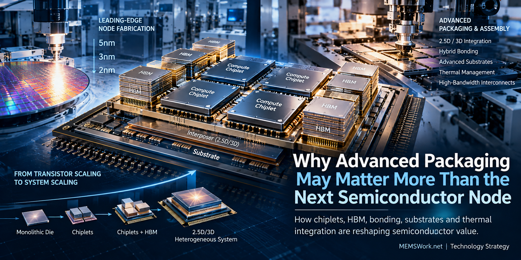
Concept illustration of advanced semiconductor packaging integrating chiplets, high-bandwidth memory, interposers, substrates and thermal-management technologies.
Why Advanced Packaging May Matter More Than the Next Semiconductor Node
Leading-edge process nodes remain fundamental, but AI is shifting value creation toward package-level integration. As accelerators combine compute dies, high-bandwidth memory, I/O chiplets and high-speed interconnects, usable performance increasingly depends on 2.5D/3D assembly, hybrid bonding, substrates, test, yield and thermal management—making advanced packaging a second scaling engine for the semiconductor industry.
From transistor scaling to system scaling
For decades, semiconductor competition could be summarized by one question: who could manufacture the smallest transistors at acceptable cost and yield? That model is becoming incomplete. Modern AI accelerators increasingly combine leading-edge compute dies, high-bandwidth memory (HBM), I/O chiplets, specialized silicon and high-speed interconnects in one package. The package is no longer just a protective enclosure; it is becoming part of the computing architecture.
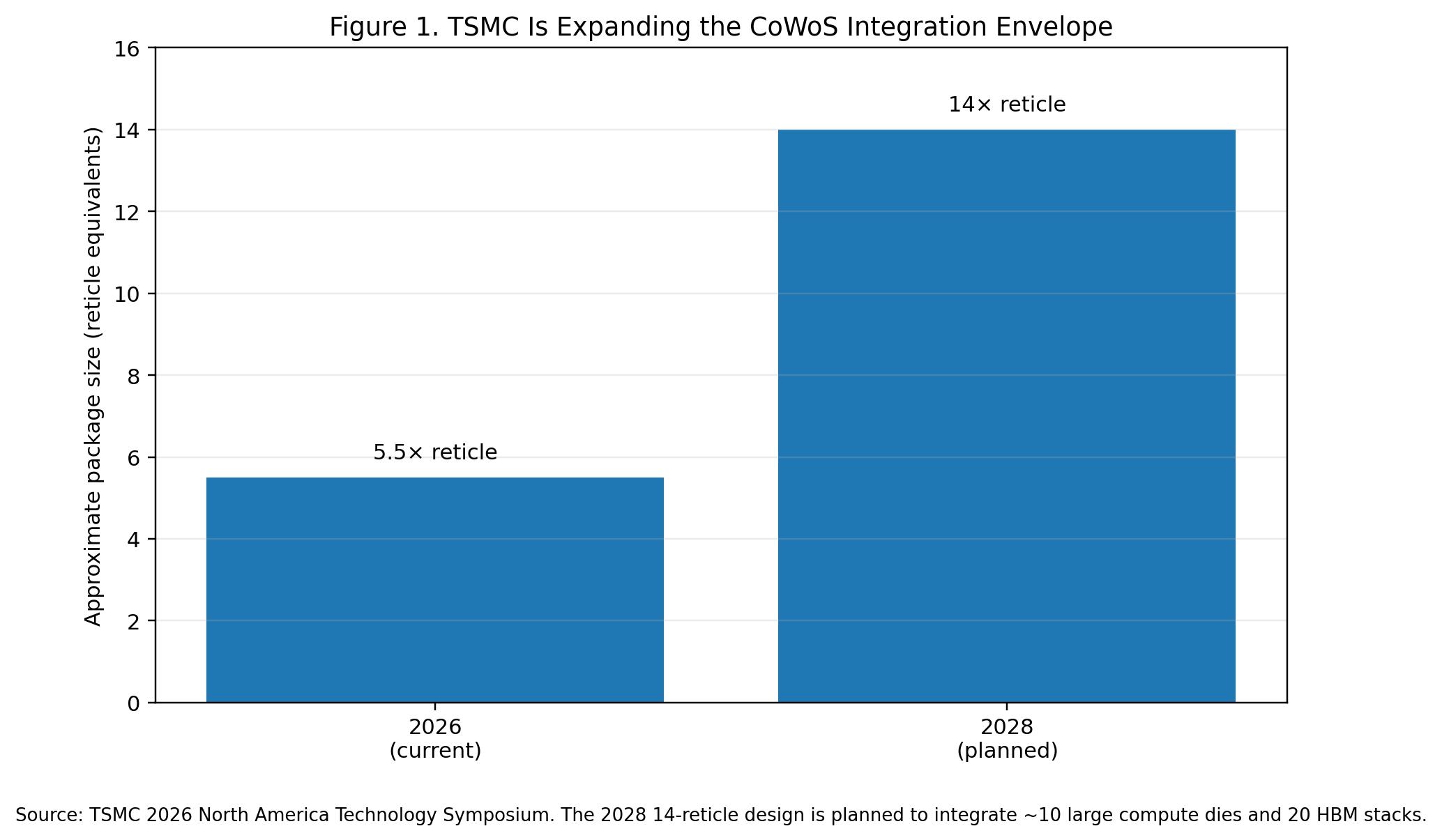
The change is visible in TSMC’s 2026 technology roadmap. The company said it was already producing 5.5-reticle-size CoWoS packages and plans a 14-reticle-size CoWoS generation in 2028 capable of integrating roughly 10 large compute dies and 20 HBM stacks. TSMC also said its N2U process enhancement, due in 2028, is designed to provide 3–4% higher speed or 8–10% lower power and 1.02–1.03 times the logic density of N2P. These are different scaling dimensions and should not be compared directly, but together they show why chipmakers increasingly need both transistor scaling and package-level integration.
Why packaging is becoming the constraint
AI processors are pushing against several limitations of monolithic semiconductor design. Very large dies approach lithography reticle limits and become increasingly sensitive to defects. HBM must sit physically close to processors to provide the bandwidth required by modern AI workloads. Meanwhile, not every semiconductor function benefits economically from fabrication on the newest logic process. Chiplets allow compute, I/O and other functions to be fabricated separately—but they transfer complexity downstream.
The result is a new constraint stack: 2.5D/3D assembly, hybrid bonding, interposers and silicon bridges, advanced substrates, test, yield and thermal management. TrendForce reported in April 2026 that AI demand had tightened not only 3 nm and 2 nm wafer capacity but also 2.5D/3D packaging, with shortages propagating into equipment, substrates and packaging materials. In September, it said growing AI-package dimensions were driving migration from CoWoS-S toward larger CoWoS-L configurations, while Intel EMIB-T was emerging as an alternative where CoWoS capacity or interposer economics become limiting.
Capital is following the bottleneck
Corporate investment provides some of the strongest evidence that packaging is becoming strategically important. TSMC raised its 2026 capital-budget guidance to $60–64 billion; approximately 10–20% is earmarked for advanced packaging, testing, mask making and related areas. CEO C.C. Wei also noted that bottlenecks can migrate between front-end and back-end operations and specifically mentioned tester shortages as one reason capital allocation must remain flexible.
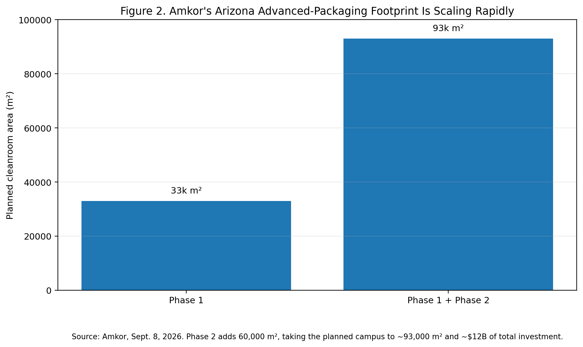
Amkor’s investments are even more explicit. The company reported record second-quarter 2026 sales of $1.90 billion, up 26% year over year, while highlighting AI and high-performance-computing programs and advanced-packaging expansion. In September, it expanded its planned Arizona advanced-packaging and test campus to approximately $12 billion. Phase 2 adds 60,000 square meters of cleanroom space to the 33,000 square meters planned for Phase 1, taking the campus to roughly 93,000 square meters.
Customers are helping finance that capacity. NVIDIA entered a $1.5 billion multi-year advanced-packaging and development agreement with Amkor, including a prepayment supporting U.S. capacity expansion. TSMC and Amkor separately signed a 10-year agreement under which TSMC can procure advanced packaging and test services from Amkor in Arizona. Intel likewise reorganized advanced packaging under dedicated leadership in June, describing packaging and system integration as defining capabilities for next-generation computing.
The constraint stack and how it can be relieved
| Constraint | Why it matters | Potential relief or innovation |
|---|---|---|
| Interposer and package size | More compute dies and HBM push packages beyond conventional reticle-scale integration. | CoWoS-L, silicon bridges, EMIB-T, fan-out panel-level packaging and system-on-wafer approaches. |
| Yield | A package may contain multiple high-value dies; late-stage defects destroy more accumulated value. | Known-good-die testing, improved metrology, inspection, bonding control and design-for-test. |
| Substrates and warpage | Larger packages increase routing-density, dimensional-stability and thermal-expansion challenges. | Advanced ABF, glass-core concepts, improved low-CTE materials and process-control tools. |
| Thermal integration | Dense logic plus HBM concentrates heat and limits sustained performance. | Advanced thermal-interface materials, microfluidic cooling, liquid cooling and package-aware thermal design. |
| Manufacturing economics | Very large packages consume wafer and interposer area inefficiently. | Panel-level packaging; ASE plans production on a 310 × 310 mm platform in 2027. |
ASE’s move toward panel-level manufacturing shows how packaging itself can become an efficiency frontier. Its automated 310 × 310 mm panel platform is expected to enter production in 2027. ASE says a 5.5-reticle-size interposer example that yields nine units on a 300 mm wafer could yield 16 on a square 310 mm panel, illustrating the potential utilization advantage.
Where innovation opportunities may emerge
The most interesting opportunities may not be in another general-purpose accelerator. They may be in enabling technologies that raise package yield or reduce the cost of heterogeneous integration: hybrid-bonding equipment, temporary bonding and debonding, wafer thinning, high-density redistribution layers, substrate materials, defect inspection, stacked-die test, warpage metrology, thermal-interface materials, co-packaged optics and chip-package co-design software. Every improvement that prevents an expensive multi-die package from being scrapped has disproportionate economic value.
Thermal engineering may become particularly important. TrendForce, citing comments from TSMC’s advanced-packaging R&D organization, reported that AI-system power could increase roughly sixfold over five years, while package size could expand from about 3.3 reticles in 2024 to more than 14 by 2029. That makes cooling and power delivery part of packaging economics rather than downstream mechanical design.
- Hybrid bonding and advanced metrology: equipment and process control that increase bond quality and detect defects earlier.
- Known-good-die and stacked-die test: tools that protect the accumulated value of multi-die systems.
- Advanced substrates and panel-level packaging: materials and formats that improve routing density, dimensional stability and area utilization.
- Thermal integration: interface materials, liquid or microfluidic cooling and package-aware thermal design.
- Co-packaged optics and co-design software: technologies that improve bandwidth, power efficiency and system-level optimization.
Investor and strategy implications
The conclusion is not that process nodes have stopped mattering. Leading-edge transistor technology remains fundamental to performance and energy efficiency. What is changing is that node scaling alone is no longer sufficient. AI performance increasingly depends on whether compute dies, HBM, I/O, interconnects, substrates and cooling can be integrated at high yield and acceptable cost.
For investors and corporate strategists, the relevant question therefore expands from who owns the next semiconductor node? to who controls the technologies that allow many expensive pieces of silicon to operate reliably as one system? The companies that solve bonding, packaging, substrate, test and thermal constraints may capture a larger share of the value created by the AI-infrastructure buildout—even if their logos never appear on the accelerator itself.
Takeaway
Advanced packaging is not replacing transistor scaling; it is becoming the second scaling engine. In AI, value increasingly depends on converting many advanced components into one high-yield, high-bandwidth and thermally viable system. The shift moves strategic attention toward the suppliers, materials, equipment, software and manufacturing methods that make heterogeneous integration economically scalable.
Sources
- TSMC, 2026 North America Technology Symposium, April 23, 2026
- TSMC, Q2 2026 Earnings Conference Call
- TrendForce, AI Competition Turns into a Supply Chain Arms Race, April 30, 2026
- TrendForce, AI Chip Packaging Pushes Beyond Reticle Limits, September 18, 2026
- Amkor Technology, Q2 2026 Results, July 27, 2026
- Amkor Technology, Arizona Phase 2 Expansion, September 8, 2026
- Amkor-NVIDIA Strategic Partnership, July 23, 2026
- TSMC-Amkor 10-Year Partnership, June 16, 2026
- Intel, Advanced Packaging Leadership Announcement, June 18, 2026
- ASE, 310 mm × 310 mm Panel-Level Packaging Platform
- ASE, Panel-Level Packaging and the Next Phase of Scaling, August 27, 2026
- TrendForce, TSMC Eyes Chip-Level Microchannel Cooling, September 2, 2026
Research note: Numerical statements are sourced to primary company materials where available. TrendForce estimates are identified as forecasts or estimates and should not be treated as company guidance.