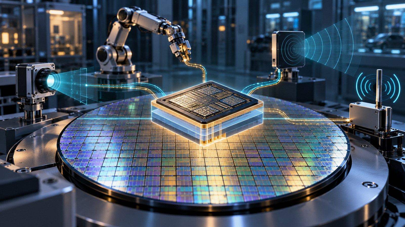
FDX Fusion: The Proof Test for Physical AI Silicon
GlobalFoundries’ FDX Fusion roadmap proposes a new kind of edge-AI foundry platform: one process that combines dense digital logic with RF, analog, embedded memory and low-power control. The strategic opportunity is real, but the label “7 nm-class” is not yet production evidence. Demo silicon, a usable design kit, qualified IP, yield and customer products will decide whether the platform becomes infrastructure for Physical AI or remains a promising roadmap.
MEMSWork Intelligence Dashboard
| Field | Assessment |
|---|---|
| Market status | Roadmap stage; demonstrator silicon is targeted for early 2027 and manufacturing for 2028. |
| Primary constraint | Turning an ambitious integration target into a stable, economical process with qualified design infrastructure. |
| Demand driver | Edge systems that must sense, infer, control and communicate within tight power, latency and safety budgets. |
| Time horizon | Design evaluation in 2027; production-readiness evidence in 2028 and beyond. |
| Technologies to watch | Adaptive body bias, embedded non-volatile memory, RF/mmWave, in-memory computing and heterogeneous integration. |
| Strategic signal | Europe is linking an open R&D pilot line, engineered substrates and expanded foundry capacity around FD-SOI. |
| Next trigger | Measured demonstrator data and a PDK that customers can use for real designs. |
Decision Question: Is FDX Fusion an Alternative to Leading-Edge FinFET?
Not as a general-purpose replacement. FDX Fusion is better understood as an attempt to make system integration, power efficiency and mixed-signal capability more valuable than maximum logic density. That distinction matters for robots, radar, industrial automation and intelligent sensors, where a processor must interact with noisy analog signals, high-voltage interfaces, radios and real-time control loops.
On October 9, 2026, GlobalFoundries announced that the first generation is expected to deliver “seven nanometer class” digital performance, more than twice the density of first-generation FDX and RF performance up to 0.5 THz fT/fmax. It also targets analog, mixed-signal, embedded non-volatile memory and in-memory computing on the same platform. The company plans demonstrator silicon for early customer evaluation in early 2027, an initial process design kit in mid-2027 and manufacturing in Dresden in 2028. These are vendor targets, not measured production results. GlobalFoundries provides the complete roadmap and schedule.
What Changed: FD-SOI Is Moving Up the Integration Curve
FD-SOI uses a thin silicon channel above a buried insulating layer. Its planar structure supports body biasing, which lets designers adjust transistor behavior after fabrication to trade performance against leakage. That capability is attractive when a device alternates between long low-power periods and short bursts of compute. It also provides a route to integrating functions that are awkward or costly to combine on a logic-only process.
The novelty is therefore not a node label alone. It is the proposed fusion of the Physical AI signal chain: sensing interfaces, local compute, memory, control and communication. This complements the software and equipment interoperability questions discussed in MEMSWork’s analysis of the model-hardware standard for Physical AI. A common hardware interface cannot compensate for fragmented silicon, and a highly integrated chip cannot compensate for weak software tooling. Commercial systems need both.
GlobalFoundries is not starting from zero. Its current FDX technology has been in volume production since 2019 and the company lists more than 700 qualified IP blocks across analog, RF, I/O, memory, power management and foundation libraries. Those figures describe the existing platform, not FDX Fusion; the new process must re-establish that breadth with silicon-proven blocks. The company’s FDX technical overview separates current capabilities from the future roadmap.
The Evidence Ladder from Roadmap to Production
| Stage | Evidence available | Commercial question still open |
|---|---|---|
| Platform definition | Targeted 7 nm-class performance, >2× first-generation FDX density and RF up to 0.5 THz fT/fmax | What are the measured PPA, variability and cost on representative circuits? |
| Demonstrator | Customer evaluation silicon targeted for early 2027 | Do SRAM, RF, analog, eNVM and compute blocks meet targets together? |
| Design enablement | Initial PDK planned for mid-2027 | Are models, rules, libraries and EDA flows accurate enough for first-pass success? |
| Manufacturing | Dresden production planned for 2028 | Can defect density, yield, cycle time and reliability support customer economics? |
| Ecosystem scale | FAMES research access, SOI substrate supply and established FDX experience | Will customers tape out differentiated products and return with follow-on designs? |
The table shows why the next twelve months matter more than the launch headline. A process can look compelling in transistor and test-chip data while still failing at the product level because models are incomplete, memory options lag, RF and digital blocks interfere, or yield makes the integrated die uneconomic.
Europe Is Building More Than a Fab
FDX Fusion sits inside a broader European technology stack. The FAMES pilot line, coordinated by CEA-Leti, runs through December 2028 and is designed to develop 10 nm and 7 nm FD-SOI generations with embedded memory, RF, power management and 3D integration. Its declared total cost is €433.6 million, including an EU contribution of €216.8 million. The project also states that forty industry organizations have signed letters of support. These are program commitments rather than production orders, but they create a shared route from research to prototypes. CORDIS documents the scope, funding and timeline.
CEA-Leti described GlobalFoundries in June 2026 as an end user of the pilot line and identified strained-silicon substrates, RF, embedded memory, compute-in-memory and heterogeneous integration as collaboration areas. That relationship is important: a foundry roadmap gains credibility when research modules can be evaluated against industrial design requirements before transfer.
Manufacturing scale is being developed in parallel. GlobalFoundries says its €1.1 billion SPRINT expansion is intended to lift Dresden capacity above one million 300 mm wafers annually by the end of 2028, from up to 950,000 wafers depending on product mix. The company also notes that FDX Fusion development under the planned IPCEI program remains subject to German federal approval. The Dresden announcement states both the capacity targets and the approval condition. Capacity, however, is not equivalent to FDX Fusion allocation, qualified output or customer demand.
Commercial Implications for Physical AI
If the integration promise holds, customers could replace several companion chips with a more tightly coupled device. Fewer die and interfaces can reduce board area, communication energy and qualification burden. The largest opportunity may be products whose value comes from trusted real-time interaction rather than benchmark leadership: automotive radar, motor control, industrial sensing, secure wireless nodes and robotic subsystems.
The counterargument is economic. Mixed-signal integration creates trade-offs. Combining functions may enlarge die area, complicate validation and concentrate failure risk. Advanced logic can also be wasteful for analog-dominant products, while chiplets remain attractive when different functions need different process technologies. The right comparison is therefore not FDX Fusion versus the fastest FinFET. It is FDX Fusion versus a credible multi-chip bill of materials, including package, interface power, software effort, qualification time and supply-chain risk.
This is similar to the manufacturing test identified in MEMSWork’s analysis of light-to-token AI vision: moving intelligence into the sensor changes where variation, calibration and model portability must be controlled. FDX Fusion could broaden that architectural option, but only if the foundry provides predictable models and production statistics.
What to Watch Over the Next 12 Months
- Demonstrator disclosure: measured logic, SRAM, analog, RF and leakage results on the same process, with temperature and voltage conditions.
- PDK credibility: named EDA support, standard-cell and memory libraries, verification flows and customer-access terms around the planned mid-2027 release.
- Customer specificity: a tapeout or product program beyond general expressions of interest, especially in radar, robotics or industrial control.
- Manufacturing evidence: defect-density trend, reliability qualification, automotive-grade options and a realistic ramp sequence for Dresden.
- Substrate resilience: multi-year supply commitments and evidence that advanced engineered substrates can scale without becoming the limiting input.
- Integration economics: customer comparisons between a single-die FDX Fusion design and a multi-chip alternative, including package and software costs.
What Would Change the Thesis?
The thesis would strengthen if customer demonstrators validate the announced performance and integration targets, the first PDK attracts real tapeouts, and Dresden reports a credible path to qualified volume production. It would strengthen further if customers disclose system-level power or cost advantages against multi-chip implementations.
It would weaken if the schedule slips materially, if the PDK lacks mature third-party IP and EDA support, or if measured density and power fall short of the “7 nm-class” framing. It would reverse if customers consistently choose mature FinFET-plus-chiplet architectures because FDX Fusion’s integrated die is more expensive, harder to qualify or less flexible.
Takeaway
FDX Fusion is strategically interesting because it treats Physical AI as a mixed-signal systems problem rather than a contest for the smallest transistor label. GlobalFoundries has aligned a roadmap, a research pipeline, substrate relationships and Dresden capacity around that idea. The evidence is still pre-production. Over the next year, demonstrator measurements, PDK quality and named customer designs will reveal whether the platform can convert European FD-SOI strength into durable product economics.
Sources and Methodology
- GlobalFoundries, FDX Fusion roadmap, October 9, 2026.
- GlobalFoundries, FDX FD-SOI technical platform overview.
- GlobalFoundries, Dresden SPRINT expansion, October 9, 2026.
- CEA-Leti, GlobalFoundries collaboration in FAMES, June 11, 2026.
- European Commission CORDIS, FAMES project fact sheet.
- GlobalFoundries and Soitec, SOI wafer supply agreements.
- GlobalFoundries, 22FDX+ production and design-win baseline.
Published October 19, 2026. Last updated October 19, 2026. Original analysis; no material revisions after publication.