


Onshoring Semiconductor Manufacturing: Bottlenecks and Investment Opportunities (II/II)
Building a domestic fab is only the first step. This Part II traces the constraints in funding, talent, packaging, utilities and yield—and identifies the operating evidence investors should watch.

The U.S. can build more semiconductor factories and still fall short of a resilient, profitable supply chain. The binding constraint moves as a project advances: from construction and skilled labor to process yield, packaging, customer qualification and utilization. Investors should follow that sequence rather than treating announced spending as finished output. This article extends Part I’s policy case by asking where production can stall and which solutions create durable value. [1]
Capacity plans are real but conditional
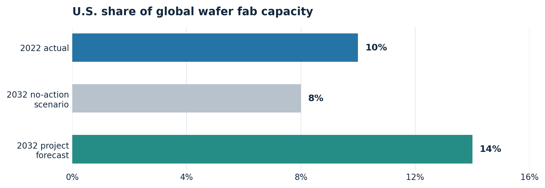
A Semiconductor Industry Association and Boston Consulting Group model published in 2024 projected that U.S. wafer-fab capacity would rise 203% from 2022 to 2032. Its forecast put the U.S. share of global capacity at 14% in 2032, against 10% in 2022 and an 8% counterfactual without new policy support (Figure 1). These are scenarios based on announced projects, not a measurement of future wafer output. Even a completed fab must be equipped, staffed and qualified before it contributes saleable chips. [2]
Why the bottlenecks persist
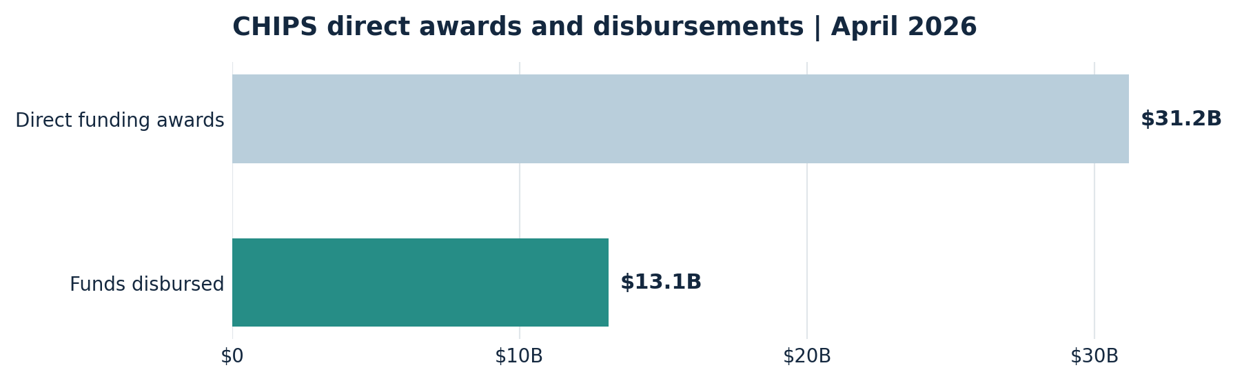
Capital arrives in stages. The Government Accountability Office reported $31.2 billion in CHIPS direct funding awards as of April 2026, with $13.1 billion disbursed—about 42% (Figure 2). Payments generally follow milestones; the undisbursed balance is therefore not evidence that projects failed. GAO nevertheless found that some anticipated milestones slipped, and two projects under one awardee were expected to finish two years later than originally agreed. An investor should separate award, disbursement, construction, tool installation and customer-qualified output. [3]
People are another rate limiter. A 2023 SIA/Oxford Economics study projected nearly 115,000 additional U.S. semiconductor jobs by 2030 and estimated 67,000 could go unfilled at then-current degree completion rates. Of that potential shortfall, 39% were technicians, 35% bachelor-level engineers or computer scientists, and 26% advanced-degree engineers. This is a scenario rather than an observed 2026 vacancy count, but it explains why cleanroom readiness cannot be inferred from a building schedule. [4]
Then comes the production ramp. TSMC said its first Arizona fab had entered volume production in late 2024, while its 2025 U.S. expansion plan included advanced packaging facilities. Those are different milestones: fabricating a wafer locally does not automatically mean the complete chip can be assembled and tested locally. GAO found in 2026 that Commerce had changed the approach to the National Advanced Packaging Manufacturing Program without a replacement plan or timeline, risking delay in a key domestic capability. [5, 3]
Economics can bind even when capacity works. Fabs carry high fixed costs, so idle tools and low yields raise cost per good die. If demand shifts after equipment is ordered, a new plant may struggle to cover depreciation and utilities. Micron’s fiscal third-quarter 2026 report shows the opposite side of the cycle: it reported $7.1 billion of net capital expenditures alongside strong AI-related memory demand. That supports investment today, but it does not guarantee that every domestic expansion will earn its cost of capital when supply catches up. [6]
Solutions and the opportunities they create
The remedies should target the constraint at each handoff. Regional colleges and employers can jointly run paid apprenticeships on actual fab tools, with portable credentials in maintenance, contamination control and metrology. Firms can also retain experienced engineers through structured transfers between mature and new sites. These measures attack ramp time directly; head-count pledges alone do not. [4]
For packaging, shared pilot lines and multi-customer qualification programs can spread the cost of substrates, bonding, inspection and reliability testing. GAO’s warning about the packaging program makes a practical case for consortia that publish common test methods and give smaller suppliers access to pilot capacity. Such facilities would lower the time and capital needed to move a promising process from lab samples to customer acceptance. [3]
Utility and materials risks call for site-level engineering: long-term power and water agreements, reuse systems, dual-qualified specialty chemicals and spares, and transparent contingency plans. Digital twins, inline sensing and statistical process control can shorten yield learning, but their value must be demonstrated in fewer excursions and more good dies per wafer. In commercial terms, customer-backed capacity reservations and phased tool purchases can reduce the risk of building ahead of demand. These are proposed approaches, not reported industry outcomes.
Where investors should look
The most interesting opportunities may sit beside the fab: process metrology, defect inspection, advanced packaging, high-purity material recycling, industrial water reuse, and training platforms tied to measurable proficiency. Each should be judged against a customer’s bottleneck and purchasing decision, not merely its exposure to “onshoring.” The test is whether it improves yield, qualification time, throughput or cash returns at a cost customers will pay.
| Constraint | Relief mechanism | Evidence to watch |
|---|---|---|
| Skills | Paid tool-specific training and mobility | Time to independent tool operation; retention |
| Packaging | Shared pilot line and common qualification | Customer approvals; package yield; lead time |
| Fab ramp | Inline metrology and defect analytics | Good dies per wafer; utilization; scrap |
| Utilities | Water reuse and firm power planning | Outages; water intensity; operating cost |
| Demand | Phased equipment and capacity contracts | Booked load; cash flow after capex |
Table 1. Proposed interventions and operating indicators. Measures are editorial recommendations, not forecasts.
The central investment distinction is between capacity on paper and capacity that customers repeatedly buy at an acceptable margin. Watch milestone dates, workforce retention, package qualification, utilization and free cash flow together. Progress on one metric without the others may shift the bottleneck rather than solve it.
References
[1] Vossough, Part I, May 2025.
[2] SIA–BCG, Emerging Resilience in the Semiconductor Supply Chain, 2024.
[3] GAO, GAO-26-109121, August 2026, data through April–June 2026.
[4] SIA and Oxford Economics, Chipping Away, 2023.
One Response