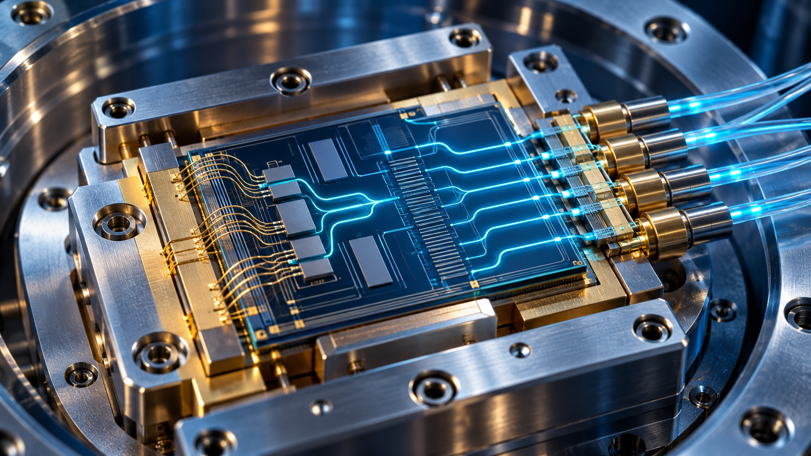
Conceptual quantum-photonic package illustration. Original MEMSWork artwork; not a vendor product or exact circuit architecture.
Quantum Photonics: The Packaging Test for Programmable Chips
Programmable quantum photonic chips are beginning to combine light generation and routing within a common device. Their commercial value will depend on preserving that functionality after optical connections, electrical controls, and operating-temperature requirements are integrated. Recent research makes packaging a concrete diligence question: can a reproducible module deliver useful quantum performance without excessive alignment, calibration, or service effort?
MEMSWork Intelligence Dashboard
| Field | Current assessment |
|---|---|
| Market status | Research demonstrations and manufacturing-platform development; no broad deployment established by this evidence. [1] [2] [3] [4] [5] [6] |
| Primary constraint | Translating integrated-device results into repeatable packaged-system performance. |
| Demand driver | More controllable quantum-light interfaces and circuits for computing and communication. [1] [3] |
| Time horizon | Platform-specific qualification; the sources do not establish a universal commercialization date. |
| Technologies to watch | Quantum-dot emitters, nanomechanical routing, fabrication-tolerant sources, optical interfaces, and cryogenic packaging. [1] [2] |
| Strategic signal | Evaluate the module and its support requirements alongside the chip. |
| Next trigger | Independent packaged-device measurements, repeatability data, and customer acceptance criteria. |
The decision question: what survives packaging?
An integrated photonic demonstration can remove a difficult device-level obstacle while leaving the product-level question unresolved. For a corporate partner or investor, the useful test is whether the same capability survives the interfaces required to operate it outside the research setup. The relevant deliverable is a reproducible module with a defined operating procedure, measurable output, and an accountable supplier.
This extends MEMSWork’s analysis of advanced packaging as a system-scaling discipline. The distinction is important: this analysis concerns quantum-light generation and control, rather than the bandwidth economics of classical AI networking. A packaging process successful in another photonics application should be treated as an engineering starting point, not automatic qualification for a quantum device.
What changed: emitters and routing operate together
An October 5, 2026 preprint from Salamon and colleagues reports a cryogenic gallium-arsenide platform combining two independently tunable quantum-dot emitters with a nano-electromechanical photon router. Separate electrical addressing permits simultaneous operation. The researchers report preservation of coherent emission, including after repeated warm-up and cooldown cycles. They identify cryogenic packaging and electrical/optical interfaces as expected scaling limitations. This is a research demonstration, not a production-qualified module. [1]
The commercial interpretation is narrower than “quantum hardware is ready.” Integration brings previously separate functions under common control and makes the interface requirements more concrete. Diligence can therefore move from isolated component promises toward a system acceptance plan. That plan should define which performance is measured, where the measurement boundary sits, and what adjustments an operator must perform before obtaining the result.
Different demonstrations remove different constraints
A September 24, 2026 preprint by Medina and colleagues describes a silicon photon-pair circuit operating without active tuning of its components. It combines generation, pump rejection, and demultiplexing using structures designed for reduced sensitivity to fabrication variation. The result addresses a different obstacle from integrating tunable emitters and routing: reducing the adjustment burden associated with matching circuit components. The accessible abstract establishes the reported demonstration; it does not establish production yield or packaged lifetime. [2]
PsiQuantum’s 2025 Nature paper benchmarks integrated silicon-photonic modules for generating, manipulating, networking, and detecting heralded qubits. Its reported fidelities are conditional on photon detection and do not account for loss. That boundary matters when converting device performance into a system argument. Successful detected events and successful operation of a complete machine are different measures. [3]
A September 21, 2026 preprint by Steiner and colleagues reports two-photon interference in a six-mode programmable circuit on a nanosatellite. It supplies evidence of integrated quantum-photonic operation in an orbital environment, rather than evidence that all quantum-photonic architectures can use the same packaging. The abstract describes generation, manipulation, and detection of non-classical light; it does not establish useful computational advantage or general-purpose quantum computing in orbit. [4]
These results should be compared by the constraint they address. A device that reduces tuning needs, a circuit that combines active functions, and a platform that operates in a demanding environment each answer a distinct question. Combining their strongest headline claims into a single hypothetical product would obscure the interfaces and qualifications still required.
| Evidence | Documented contribution | Maturity | Proposed qualification question |
|---|---|---|---|
| Integrated active functions | Cryogenic quantum-dot emitters and nanomechanical routing share control infrastructure. [1] | Research device | Does the packaged configuration preserve concurrent operation? |
| Reduced tuning burden | Passive silicon photon-pair circuit avoids active component tuning in the reported experiment. [2] | Research device | How repeatable is performance across fabricated and assembled devices? |
| Manufacturing platform | Integrated photonic modules are benchmarked; fidelity values condition on detection and exclude loss. [3] | Platform demonstration | What is the complete module’s loss and acceptance boundary? |
| Environmental operation | Programmable quantum-photonic operation is reported on a nanosatellite. [4] | In-orbit demonstration | Which qualification conditions apply to the intended architecture? |
Table 1. Quantum-photonic demonstrations address different integration constraints. Documented contributions and maturity derive from sources [1] [2] [3] [4]. Qualification questions are MEMSWork synthesis; the rows are not a performance ranking.
Packaging diligence should follow the measurement boundary
MEMSWork’s proposed review begins at the optical boundary. Request measurements from the assembled module’s input to its usable output, alongside the chip-level result. Ask which connections, filters, and detection conditions are included. Record how much adjustment is required to reproduce a result after installation or a thermal cycle. Establish whether the reported output includes unsuccessful trials or conditions on a selected subset of events.
Next, examine the control boundary. Require a documented map of electrical connections, operating procedures, and the responsibilities of the chip, package, controller, and cooling suppliers. Evaluate changes in the intended configuration rather than accepting every subsystem’s standalone pass as proof of a system pass. A useful acceptance exercise would repeat the relevant optical measurement while operating the complete control configuration.
Finally, connect those tests to a manufacturing boundary. Ask for distributions across multiple devices and builds, the disposition of failed assemblies, and the steps that require manual intervention. Define traceability from a packaged result back to its die, assembly process, and calibration record. These are proposed diligence requirements, not claims that the cited teams have completed or failed such tests.
Foundry progress and module readiness need separate evidence
Imec’s March 13, 2026 announcement describes transferring its low-pressure chemical-vapor-deposition silicon-nitride photonics platform to New Origin and scaling manufacturing on 200 mm wafers. The collaboration targets several applications, with quantum among them. It supports evidence of an industrialization effort; it is not a guarantee that a particular quantum design already has qualified volume manufacturing. [5]
SRI’s June 29, 2026 announcement of the NIST-backed Quantum Manufacturing Engineering Center identifies cryostats and lasers as initial focus areas, alongside scalable processes, quality control, and supply-chain development. This is an institutional manufacturing initiative rather than a customer deployment result. It reinforces the relevance of enabling components without establishing a market forecast or assured commercial demand. [6]
For a procurement team, the proposed implication is to qualify the process chain explicitly. Which organization supplies the photonic die, who assembles the module, and who owns the final acceptance test? MEMSWork’s supplier-qualification analysis provides a related framework for those responsibilities. The technology platform and the packaged product should have separate evidence files.
Where suppliers can create defensible value
The proposed opportunity is to remove a verified integration burden. Optical attachment, control electronics, package characterization, calibration tools, and specialized test can be valuable when they improve a customer’s accepted result or reduce the effort required to reproduce it. A supplier should demonstrate that improvement against a named application and operating procedure, rather than infer revenue potential from interest in quantum computing.
Commercial diligence should distinguish engineering services from a repeatable product. Ask what changes between customers, what portion of delivery is manual, and whether acceptance depends on a small group of specialists. Model assembly rework, test time, installation, and service together. A component with impressive optical specifications may still need a business model that accommodates expensive integration work.
The adjacent co-packaged-optics analysis illustrates why packaging and serviceability deserve attention in photonics. The analogy concerns qualification discipline; it does not imply that quantum modules share the same architectures, customer requirements, or market scale as AI network switches.
What to Watch Over the Next 12 Months
Look for follow-on reports that measure packaged performance, identify the operating boundary, and disclose repeatability across devices and assemblies. Track whether integrated functions continue operating together after installation and thermal cycling. Seek explicit loss accounting and calibration procedures, together with a clear explanation of any selected or conditional measurements.
Monitor foundry process access, packaging design rules, and test services that a customer can actually use. Customer-qualified modules, documented acceptance milestones, and reduced dependence on manual alignment would strengthen the commercialization evidence. Institutional programs are worth following for delivered tools and manufacturing methods, rather than treating their launch announcements as product validation.
What Would Change the Thesis?
The packaging thesis would strengthen if reproducible module data show that the main performance penalty or operating burden arises at the interfaces, and a supplier demonstrably removes that burden. It would weaken if intrinsic source or circuit limitations dominate the assembled result, leaving packaging improvements with little effect. A simpler architecture delivering the required function with lower integration effort would also challenge the proposed opportunity.
The immediate strategic task is to identify the measurement that matters to the intended customer and qualify the entire path that produces it. Recent demonstrations make that conversation more specific. Investment conviction should increase when the evidence moves from an impressive chip to a repeatable module and an accepted application.
Sources and methodology
The assessment uses the accessible Salamon manuscript, the Medina and Steiner preprint abstracts, the PsiQuantum paper’s published summary, and primary institutional announcements. Preprints are research reports; manufacturing initiatives are stated plans. No production yield, packaged lifetime, shipment volume, or market size is inferred. The comparison table and diligence questions are MEMSWork synthesis, not a matched performance ranking.
[3] PsiQuantum team, A manufacturable platform for photonic quantum computing, Nature, 2025.
[5] Imec, New Origin collaboration to scale photonic IC manufacturing, March 13, 2026.
[6] SRI, NIST taps SRI to establish the Quantum Manufacturing Engineering Center, June 29, 2026.
Last updated October 12, 2026 Pacific. Update history: Initial assessment published. Future updates should record packaged measurements, qualification milestones, and changes in the operating assumptions.