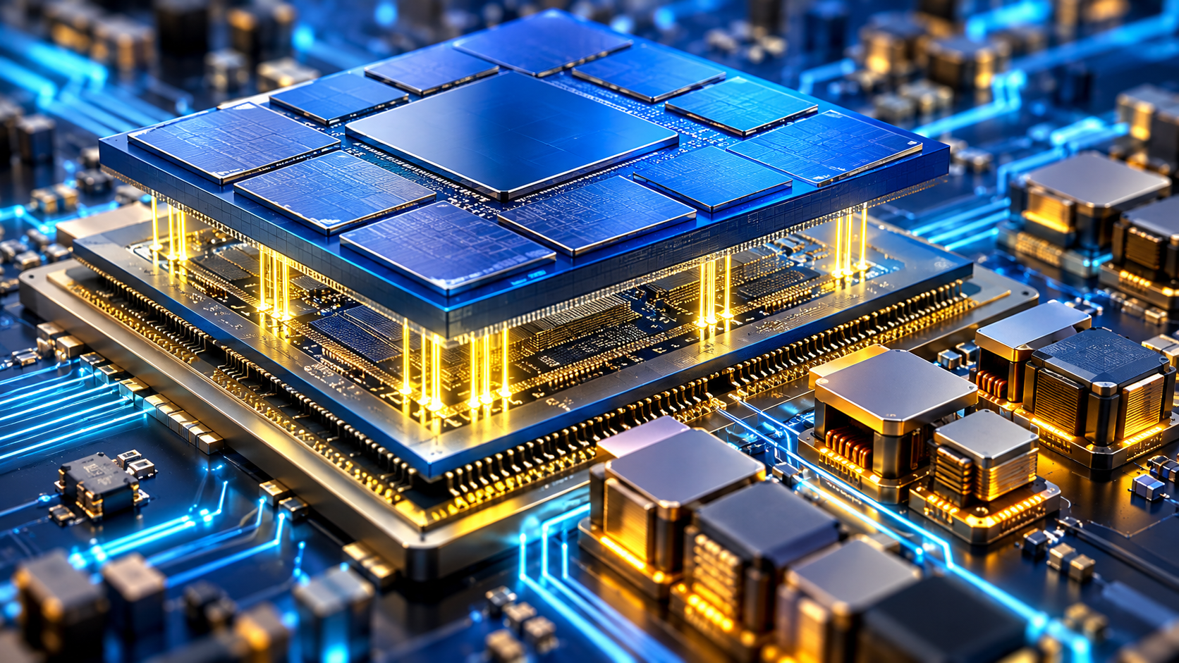
Conceptual package power illustration. Original MEMSWork artwork; not a product depiction or exact circuit architecture.
AI Chiplet Power Delivery Becomes a System Design Constraint
AI chiplet packages need power architectures designed alongside compute, memory, and cooling. Recent research and supplier developments show voltage conversion moving closer to the load, while backside power adds another integration layer. The commercial test is whether these choices preserve useful performance under changing workloads without shifting excessive cost, heat, or reliability risk into the package.
MEMSWork Intelligence Dashboard
| Field | Current assessment |
|---|---|
| Market status | Commercial supplier activity and foundry offerings coexist with research on future multi-kilowatt integration. [1] [2] [3] |
| Primary constraint | Delivering stable local voltage while accommodating conversion heat, interconnects, and assembly limits. |
| Demand driver | Higher useful AI compute within increasingly integrated packages. |
| Time horizon | Platform-specific design and qualification; no universal adoption date established. |
| Technologies to watch | Vertical power delivery, integrated regulators, embedded passives, backside power, and multiphysics design. [3] [5] |
| Strategic signal | Power architecture should be evaluated before fixing the chiplet floorplan. |
| Next trigger | Customer-qualified systems with measured workload efficiency, transient response, and reliability. |
Decision question for AI chiplet designers
How much of an accelerator’s promised performance remains usable after the power network, voltage regulators, cooling, and package assembly are included? That is the relevant purchasing question. A design can provide abundant compute capacity yet require operating margins that reduce its practical value. The proposed diligence approach is to evaluate the completed power path against the intended workload, rather than accept an isolated component specification as the system result.
This extends MEMSWork’s analysis of advanced packaging as a scaling engine. The distinct issue here is the electrical architecture inside and around the package. The data-center power infrastructure problem concerns energizing capacity; package power design determines how effectively that capacity reaches the switching circuits.
What changed in package power delivery
A University of Minnesota manuscript posted on September 21, 2026 maps design methods for future multi-kilowatt heterogeneous systems. It emphasizes coordinated voltage regulation, power distribution, thermal analysis, and reliability. This is a methodology and research agenda, not a demonstration that an arbitrary multi-kilowatt chiplet package has been qualified for production. [1]
A separate commercial signal arrived on September 17, 2026: Vicor announced a non-exclusive vertical power delivery license to an unnamed AI OEM. The announcement supports evidence of licensing activity, while leaving shipment volumes, customer economics, and comparative performance undisclosed. Its patent and licensing statements are the supplier’s position; they do not establish a universal requirement for every competing architecture. [2]
Together, these developments justify closer technical diligence. They do not justify a market-size forecast or an assumption that all accelerators will converge on one regulator placement. The useful question is which constraints a particular implementation removes and which new dependencies it introduces.
Voltage conversion and current paths must be designed together
The Minnesota analysis describes distributing power at an intermediate bus voltage and performing further conversion near the chiplets. Lowering that bus voltage can improve the local converter while raising distribution current and resistive losses. Moving regulators closer to the load shortens the demanding low-voltage path but consumes scarce physical and thermal resources. [1]
Texas Instruments supplies a concrete architecture example. Its March 16, 2026 announcement describes reference designs converting 800 V to 6 V and then to below 1 V for GPU cores. TI reports 97.6% peak efficiency for the bus converter. That figure concerns a conversion stage under specified conditions; it is not end-to-end accelerator efficiency or a guarantee at every load. [7]
The evaluation should therefore retain the boundaries around each measurement. Ask for the converter efficiency curve, distribution losses, cooling conditions, and the workload used to exercise the package. A peak result can be useful for component selection while remaining insufficient for system economics. Compare alternatives at a common useful-compute outcome, with the same operating constraints and an explicitly defined power measurement point.
Backside power complements package integration
Intel’s foundry brief connects PowerVia backside routing with on-die decoupling, EMIB-T bridges containing through-silicon vias and capacitors, and substrate-integrated inductors for voltage regulation. TSMC’s A16 description also combines nanosheet transistors with backside power rails. These are related approaches across different integration levels, rather than interchangeable product specifications. [3] [4]
Backside power changes how supply connections reach devices within silicon. Vertical package power changes where conversion and high-current connections sit relative to the processor. Either may help a design, but one does not automatically establish that the other’s constraints have been resolved. Buyers should request a complete stack description, including which elements are available today and which remain roadmap features.
| Integration choice | Documented role | Proposed qualification question |
|---|---|---|
| Local voltage conversion | TI reference architecture converts a high-voltage bus to a local bus and then core voltage. [7] | Are conversion losses measured across the intended load range? |
| Vertical package delivery | Vicor reports licensed VPD technology; Intel describes vertical connections in EMIB-T. [2] [3] | Can the assembly meet electrical and thermal requirements together? |
| Backside silicon routing | TSMC A16 and Intel PowerVia introduce backside supply routing. [3] [4] | Are device interfaces and protection validated in the final stack? |
Table 1. Power delivery choices operate at different integration levels. Documented functions come from supplier sources [2] [3] [4] [7]; qualification questions are MEMSWork synthesis, not a matched performance ranking.
Table 1 shows why supplier comparisons need an architectural boundary. A bus converter, a package connection, and a silicon power rail solve different parts of the problem. A purchasing team should map how they fit together before comparing headline claims.
Manufacturing and protection remain part of the electrical design
Imec’s backside integration work identifies wafer thinning, bonding distortion, via alignment, and metal compatibility as important process concerns. Its thermal discussion also considers how backside metal can spread heat after silicon thinning. These are implementation-specific findings, not evidence that every backside process has identical tolerances or thermal behavior. [5]
Imec’s separate ESD study gives a useful warning against treating thinning as a purely geometric change. Electrostatic discharge protection devices on extremely thin substrates can lose robustness because heat dissipates less effectively. The researchers also investigate backside contacts and metallization as mitigation paths. Those device results should inform qualification questions, without being translated into an assumed field failure rate for a vendor’s finished product. [6]
A sensible qualification plan should connect process variation with electrical margin and protection behavior. Ask who owns the acceptance criteria when a foundry, substrate supplier, regulator vendor, and assembly partner contribute different pieces. Characterization should include the assembled package, because a collection of passing components does not by itself demonstrate a passing system.
Commercial opportunity depends on verified system value
For corporate strategists, the opportunity lies in reducing a customer’s demonstrated integration burden. Embedded passives, current sensing, package characterization, and design tools deserve attention when they improve measurable performance or shorten a verified qualification process. Their attractiveness should be established through customer evidence and manufacturing capability, rather than inferred from the growth of AI alone.
For venture diligence, request an application-specific reference design, reproducible test data, supplier responsibilities, and a path to customer acceptance. Licensing activity is useful evidence of commercial engagement, but should be evaluated separately from product revenue. The relevant economic model should include assembly yield, test effort, cooling requirements, and replacement or redesign costs. MEMSWork’s supplier qualification analysis provides the broader context for that review.
What to Watch Over the Next 12 Months
Track customer-qualified implementations that report sustained performance and power at the same measurement boundary. Look for published efficiency curves, workload-dependent voltage behavior, package-level thermal maps, and reliability data. Monitor whether foundry documentation identifies production-supported power interfaces and whether regulator suppliers provide models that designers can use in the complete package flow.
Revisit the distinction between supplier announcement, reference design, and customer deployment. Named design wins with disclosed qualification milestones would strengthen the commercial evidence. Manufacturing data and customer support arrangements would be more useful than another isolated peak-efficiency claim.
What Would Change the Thesis?
The thesis would strengthen if closer integration demonstrably improves useful compute per unit of system input power while preserving electrical margin, manufacturability, and lifetime requirements. It would weaken if added conversion heat, protection changes, or assembly complexity erase the benefit. A well-qualified conventional architecture achieving the same outcome at lower total cost would also challenge the case for migration.
The decision should remain application-specific. Power delivery belongs in early system design because its constraints can alter the feasible package. Investment becomes compelling when a supplier can resolve those constraints with evidence that survives customer qualification.
Sources and methodology
The analysis uses the accessible Minnesota manuscript, foundry technical materials, supplier announcements, and imec research explanations. Vendor specifications and licensing statements remain attributed claims. No customer shipment volume, production yield, total package savings, or market forecast is inferred. The table and proposed diligence tests are original MEMSWork synthesis. The cover is conceptual artwork, not a device cross-section.
[1] Yue et al. Toward Multi kW Power Delivery Methodologies for Advanced 3D Heterogeneous Integration.
[2] Vicor licenses VPD to a leading AI OEM.
[3] Intel Foundry Accelerating HPC and AI with advanced process and packaging technologies.
[4] TSMC A16 technology.
[5] Imec How to power chips from the backside.
[6] Imec Protecting thin substrate CMOS against ESD events.
[7] Texas Instruments 800 VDC power architecture with NVIDIA.
Last updated October 9, 2026 (Pacific). Update history: Initial publication; thesis to be revisited against customer qualification, system measurements, and manufacturing evidence.