
Conceptual silicon patterning and etch equipment. Original MEMSWork illustration; not an AlixLabs product photograph or a representation of measured nanoscale geometry. [1] [5]
Atomic Pitch Splitting Enters the Manufacturing Flow
Atomic pitch splitting could simplify how semiconductor manufacturers create dense patterns. AlixLabs’ evaluation within the NanoIC pilot line creates a route to test that proposition under more demanding conditions. The decision now turns on process integration: whether attractive structures can become a repeatable manufacturing module with acceptable defects, throughput and operating cost. Equipment availability and production qualification remain separate milestones. [1] [2] [3]
MEMSWork Intelligence Dashboard
| Field | Assessment |
|---|---|
| Market status | Evaluation equipment offered; industrial process qualification remains in progress. [2] [3] |
| Primary constraint | Preserving pattern quality across wafers and operating conditions. [1] |
| Demand driver | Simpler routes to dense patterns within existing lithography flows. [1] [2] |
| Time horizon | Pilot evaluation underway; high-volume adoption timing is unproven. [1] [3] |
| Technologies to watch | Atomic layer etching, nanoimprint integration, metrology and automated chamber platforms. [1] [2] [5] |
| Strategic signal | Tool engineering and process evidence must advance together. [1] [2] [3] |
| Next trigger | Published wafer-scale results and customer-relevant equipment acceptance data. [1] |
MEMSWork synthesis based on the NanoIC evaluation announcement, Sax Forma launch and Beta assembly update. Adoption timing is an uncertainty, not a forecast. [1] [2] [3]
What changed: a pilot-line evaluation, not a production release
On October 1, 2026, AlixLabs announced a six-month evaluation of Atomic Layer Etching Pitch Splitting, or APS, within NanoIC, the pilot line coordinated by imec. The program starts with characterized line-and-space structures, develops processing on coupons and transfers selected conditions to full wafers. Its stated measurements include critical-dimension uniformity, line roughness, pitch walking, profiles and stochastic defects. [1]
That sequence matters because a patterning technique becomes commercially useful only when its operating window is understood. A successful coupon can identify a promising recipe. It cannot establish how that recipe behaves across a wafer, after chamber maintenance or when incoming structures vary. The central decision question is therefore whether APS can earn a place in a qualified process flow. [1]
The European Commission describes NanoIC as infrastructure for testing technologies at near-industrial scale before mass production. Access to that environment is a useful development signal. It does not establish a customer purchase, production yield or commercial adoption. [4]
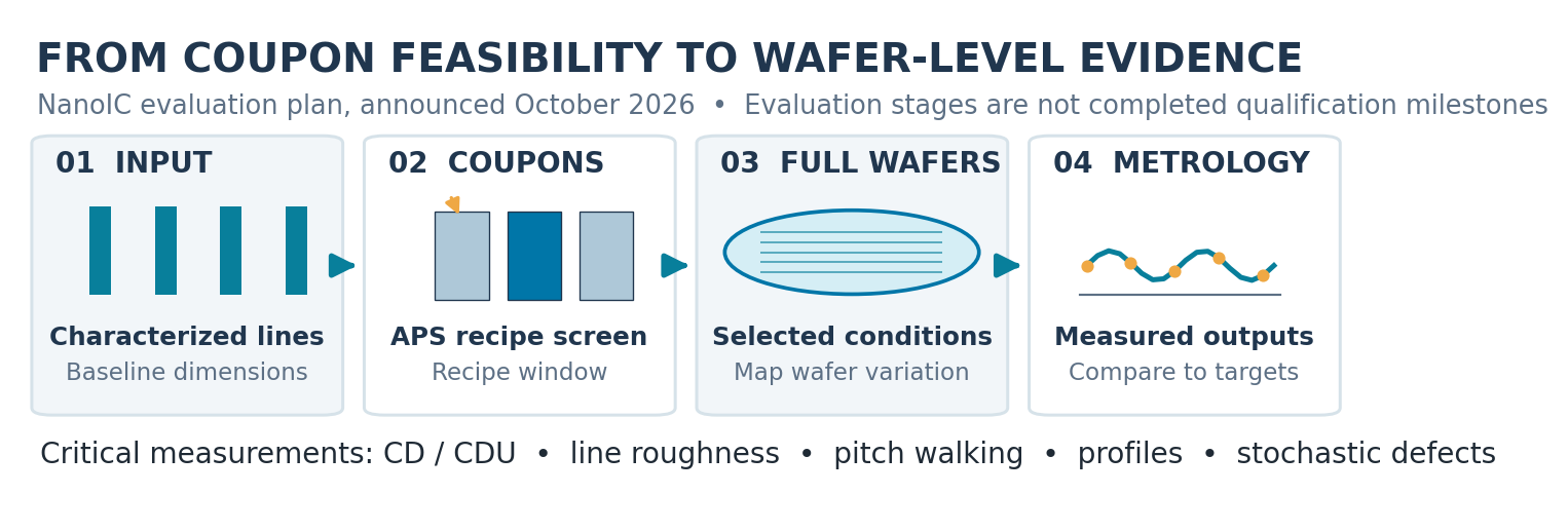
Figure 1. NanoIC evaluation sequence, as announced October 1, 2026: characterized input patterns, coupon development, selected full-wafer transfer and metrology. These are evaluation stages, not completed production qualification. [1]
How atomic pitch splitting changes pattern multiplication
Semiconductor patterning starts with a designed geometry and must transfer it into physical materials. When the desired pattern becomes denser than an initial exposure conveniently delivers, manufacturers can use additional pattern-multiplication steps. The value of a new technique depends on the complete flow it can replace or simplify. [1] [5]
Kanarik and colleagues’ review of atomic layer etching explains the underlying approach: sequential, controlled surface reactions remove thin layers of material. APS uses etching to divide prepatterned structures and increase pattern density. AlixLabs positions it as a downstream complement to lithography, including deep-ultraviolet, extreme-ultraviolet and nanoimprint approaches, in its Sax Forma launch materials. [1] [2] [5]
This complementarity changes the strategic comparison. An APS module need not displace an exposure-tool ecosystem to be valuable. It must offer a better local solution for a particular layer and material stack. Equally, fewer named process steps cannot by itself prove lower cost: cycle duration, consumables, inspection, rework and yield all remain part of the calculation. [1] [2] [5]
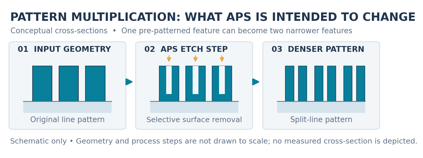
Figure 2. Conceptual APS mechanism. Selective atomic-layer etching can divide pre-patterned structures to form denser lines. Original MEMSWork schematic based on the AlixLabs technology description; not a measured cross-section or a scale drawing. [1] [5]
What the measured evidence actually establishes
A SPIE paper by AlixLabs and Canon researchers reports nanoimprint-defined silicon structures with an initial half-pitch of 26 nm, followed by APS results with a 10 nm critical dimension and a 12 nm half-pitch. The abstract gives line-edge roughness as 1.7 nm; the results section reports an average of 1.72 nm. Those are differently rounded descriptions of the reported measurement, rather than independent results. [6]
Critical dimension describes feature size; half-pitch describes half the repeating pattern period. They should not be treated as interchangeable metrics or translated into a commercial process-node claim. The paper demonstrates structural patterning. It does not establish transistor performance, electrical yield or qualified production economics. [6]
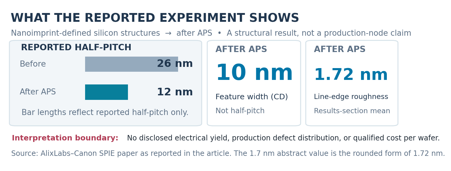
Figure 3. Published patterning experiment summarized in the article: 26 nm starting half-pitch, 12 nm half-pitch and 10 nm CD after APS; reported line-edge roughness 1.72 nm (rounded to 1.7 nm in the abstract). Source: AlixLabs–Canon SPIE paper. Not manufacturing yield data. [6]
| Evidence | What is established | What still needs proof |
|---|---|---|
| Patterning experiment | Reported 10 nm critical dimension and 12 nm half-pitch after APS on nanoimprint-defined silicon. [6] | Representative device integration and statistically useful defect distributions. |
| NanoIC evaluation | A defined program extending from coupons to selected full-wafer conditions. [1] | Completed results against a declared acceptance window. |
| Sax Forma Beta | Equipment offered for customer evaluation and production-like validation. [2] [3] | Customer acceptance, sustained operation and repeatable throughput. |
| Gamma roadmap | A high-volume platform targeted for 2028 by the vendor. [2] [3] | Delivered capability, qualified processes and recurring production use. |
Table 1. Evidence-to-decision map. Sources: SPIE patterning paper; NanoIC program; Beta launch and Gamma target. Final-column requirements are MEMSWork analysis, not reported failures. [1] [2] [3] [6]
The distinction in Table 1 is important for technical diligence. Resolution establishes feasibility. Qualification establishes where that feasibility survives the variation and constraints of a real manufacturing flow. [1] [6]
The constraint moves from geometry to process control
Uniformity should be evaluated as a distribution, not a hero image. A buyer should request the spatial pattern of dimensional variation and how it changes with incoming geometry. Roughness measurements also need a consistent method and comparable sampling. A favorable average can obscure a tail that matters to device performance. [1]
Pitch walking, an alternating departure from the intended spacing, deserves particular attention in a splitting process. As an engineering inference, systematically unequal spaces could propagate into later pattern transfer even when average pitch appears acceptable. The practical requirement is a toleranced result after relevant downstream processing, not merely after the APS step. [1]
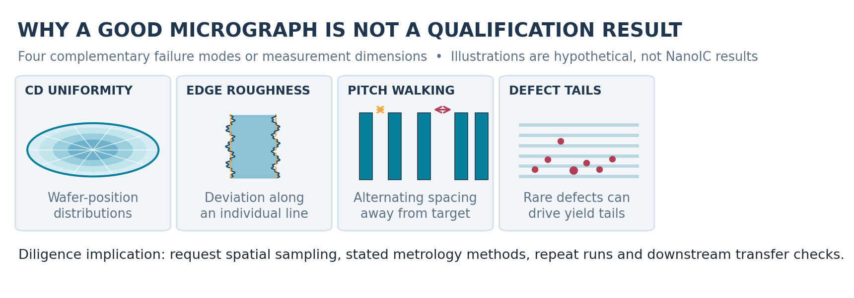
Figure 4. Why wafer-scale distributions matter. Critical-dimension uniformity, line-edge roughness, pitch walking and defect tails are illustrated schematically; no plotted values are measured APS or NanoIC results. Original MEMSWork graphics. [1]
Equipment behavior introduces another set of questions: recipe portability, chamber conditioning, particle contribution, cleaning intervals and recovery after intervention. These are diligence questions, not evidence that APS performs poorly. Their importance follows from the buyer’s need to reproduce an accepted process rather than reproduce a single experimental image. [1] [2] [3]
This is the manufacturing counterpart to MEMSWork’s analysis of supplier qualification in advanced packaging: a technically credible component becomes valuable through reliable interfaces, documented operating limits and reproducible delivery. [7]
Commercialization requires both a tool and an integration partner
AlixLabs’ June 23, 2026 launch described Sax Forma Beta as commercially available equipment for evaluation, integration and validation in production-like environments. Its August 28, 2026 update said the first Beta chamber had entered final assembly at VDL Projects, with installation in AlixLabs’ cleanroom planned by year-end. These statements describe different milestones; availability should not be read as a verified installed customer fleet. [2] [3]
The April 7, 2026 memorandum with VDL ETG Projects addresses equipment development and manufacturing. That partnership places industrial tool engineering alongside process invention. An equipment supplier can help convert a recipe into a serviceable platform, while a semiconductor integration partner determines whether the module fits a useful layer, material and downstream sequence. [8]
For corporate strategy teams, the best early engagement would be a bounded evaluation with explicit acceptance criteria and a baseline flow. For investors, the useful commercial evidence would include repeat evaluations progressing to tool acceptance and a credible service model. Pilot participation alone cannot answer those questions. [1] [2] [3] [8]
Economics should be measured per accepted output. A shorter flow may reduce complexity, but slower processing or additional inspection could offset the benefit. Published matched-flow cost and yield data remain insufficient here to quantify savings. This echoes the systems perspective in MEMSWork’s analysis of packaging versus process-node progress: a local technical advance earns its value through the surrounding system. [9]
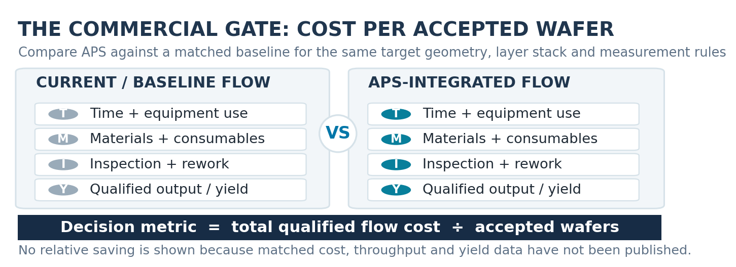
Figure 5. Comparative economic diligence framework. APS must be evaluated against a matched baseline using full-flow costs and accepted output; no cost advantage is assumed without comparable throughput and yield evidence. Original MEMSWork analysis. [1] [2] [3] [6] [9]
What to Watch Over the Next 12 Months
Watch for completed NanoIC results with declared sampling, incoming structures and acceptance criteria. Wafer maps and defect distributions would be more decision-relevant than another best-case micrograph. Disclosure of downstream pattern transfer would strengthen the bridge from geometric demonstration to integration. [1]
Track the Beta platform’s installation and acceptance milestones against the vendor’s published assembly roadmap. Automated processing, repeat runs after chamber interventions and evidence of customer qualification would clarify equipment readiness. Treat announced delivery plans as plans until completion is documented. [3]
Finally, look for a named use case with a matched baseline: the same target geometry, comparable material stack and consistent metrology. A credible demonstration of throughput and accepted yield alongside process simplification would make the economic argument testable. [1] [6]
What Would Change the Thesis?
The current thesis is that APS merits application-specific evaluation while manufacturing readiness remains unproven publicly. It would strengthen with independently characterized, repeatable full-wafer results and customer acceptance of the equipment under a declared operating window. [1] [2] [3] [6]
It would weaken if dimensional variation, defects or added inspection consumed the advantage of simplifying the flow. It would also narrow if usable results depended on starting geometries that prospective applications could not supply economically. Conversely, a qualified downstream integration with measured cost per accepted wafer would justify moving the analysis from process promise to an adoption case. [1] [6]
Sources and methodology
This analysis uses the linked NanoIC announcement, AlixLabs launch and assembly disclosures, the VDL memorandum, the SPIE research paper, the foundational ALE review and the European Commission’s NanoIC description. Company schedules and commercialization statements are attributed to their issuers. The SPIE authors include company researchers; their structural results are not independent production qualification. No market-size, cost-saving or adoption estimate has been constructed. Figures 1, 2, 4 and 5 are original MEMSWork schematics or decision frameworks based on the indicated sources, not experimental data. Figure 3 reproduces published numerical findings as an original chart and does not depict independently verified manufacturing performance.
References
[2] AlixLabs. “AlixLabs launches Sax Forma for the Ångström era.” June 23, 2026.
[3] AlixLabs. “AlixLabs Sax Forma Beta Chamber Enters Final Assembly at VDL Projects.” August 28, 2026.
Last updated: October 23, 2026. Initial publication. Future material updates should distinguish measured integration results from equipment and customer announcements.